

Large-area single-crystal monolayer graphene film and method for producing the same
a single crystal, graphene film technology, applied in envelope/bag making machinery, paper/cardboard containers, semiconductor/solid-state device details, etc., can solve the problem of difficult commercialization of graphene film, inefficient production of graphene film on a large area, and inability to grow graphene into single crystals over large area
Inactive Publication Date: 2016-04-21
IUCF HYU (IND UNIV COOP FOUNDATION HANYANG UNIV)
View PDF1 Cites 19 Cited by
- Summary
- Abstract
- Description
- Claims
- Application Information
AI Technical Summary
Benefits of technology
The present invention provides a method for producing a high-quality large-area graphene thin film of good quality, suitable for use in various applications such as transparent electrodes, display devices, semiconductor devices, separation membranes, fuel cells, solar cells, and sensors. The method involves forming a single-crystal metal catalyst layer on a substrate and then growing a graphene layer on top of the catalyst layer. The catalyst layer is made with a crystal plane orientation of (111). The invention allows for the production of large-area graphene films on a commercial scale.
Problems solved by technology
According to a general CVD method for producing a graphene film, it is known that graphene deposited on a polycrystalline transition metal catalyst layer cannot be grown into a single crystal over large area.
However, the formation of the single-crystal transition metal catalyst layer necessitates the use of the expensive single-crystal substrate, which makes the production of the graphene film on a large area economically inefficient.
Therefore, the graphene film is difficult to commercialize.
However, the substrate is essentially required and the transition metal catalyst layer crystallized by annealing is not grown into a high-quality large-area single-crystal monolayer graphene film due to its lack of a single-crystal structure, which makes it difficult to commercialize the graphene film.
The limited area of the copper foil is an obstacle to the commercialization of the single-crystal monolayer graphene film.
However, a single-crystal structure of the graphitization catalyst is not attained under the preliminary annealing conditions.
The monolayer graphene film had a single-crystal structure as a determinant of high quality but could not be produced over a large area.
Method used
View moreImage
Smart ImageViewing Examples

Examples
example 1
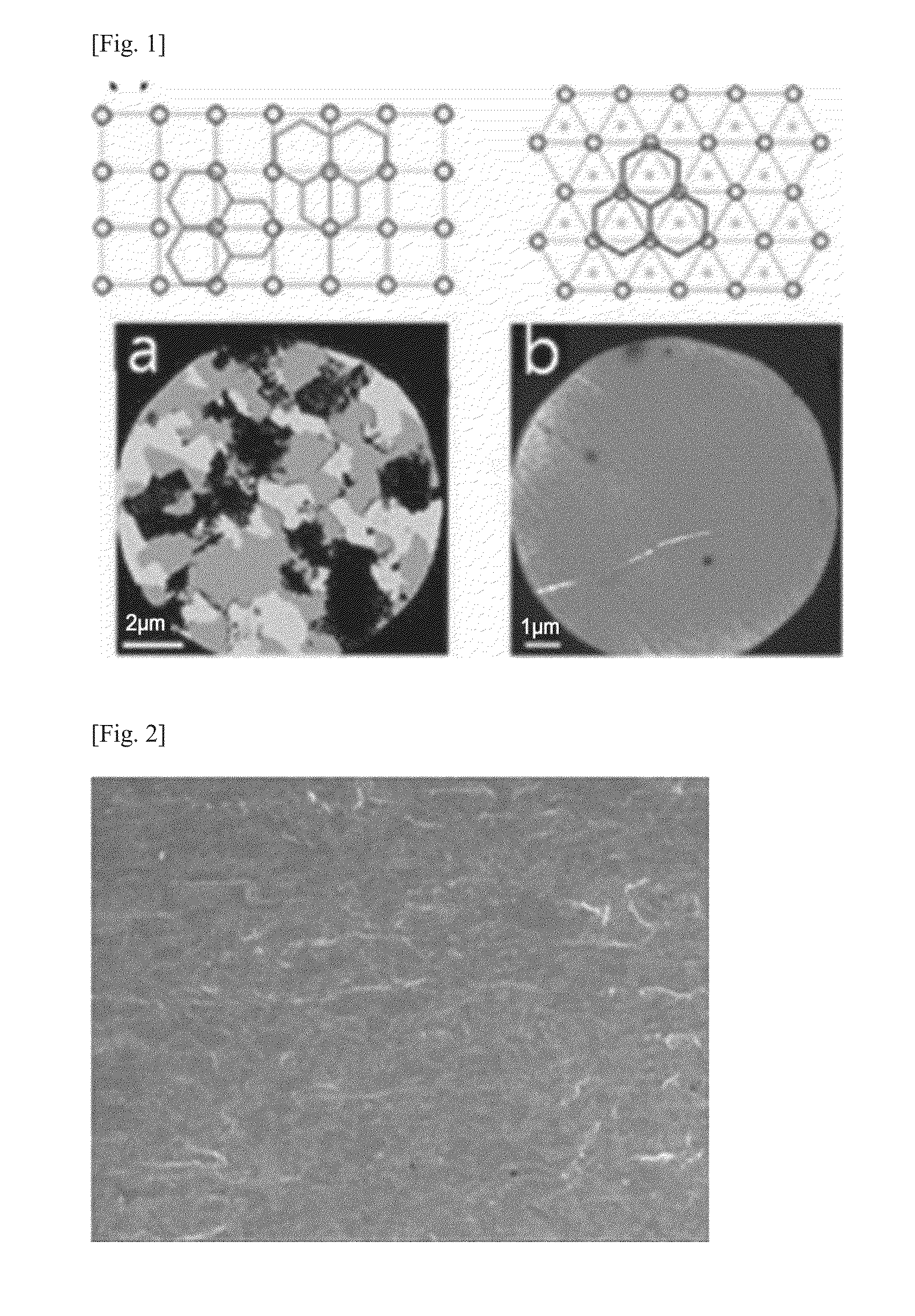
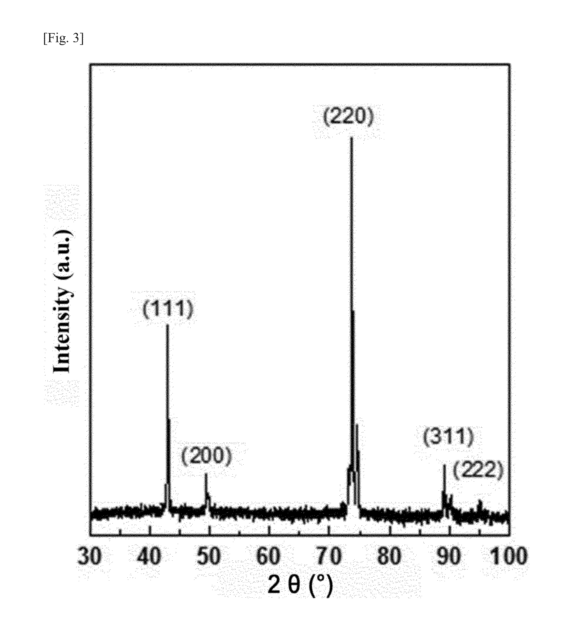
[0084]An 18 μm thick, 10 cm wide, and 10 cm long copper foil (HOHSEN, 99.9%, Japan) as a metal precursor was introduced into a chamber. The copper foil was annealed while feeding 100 sccm of hydrogen into the chamber at 1,005° C. and 500 torr for 2 h. As a result of the annealing, a copper catalyst layer was formed. Simultaneously, chemical vapor deposition (CVD) was performed while feeding a mixed gas of hydrogen (5 sccm) / methane (20 sccm) into the chamber at 1,005° C. and 0.5 torr for 60 min. As a result, a graphene layer was formed on the copper catalyst layer.
Login to View More PUM
| Property | Measurement | Unit |
|---|---|---|
| Temperature | aaaaa | aaaaa |
| Thickness | aaaaa | aaaaa |
| Thickness | aaaaa | aaaaa |
Abstract
The present invention relates to a large-area single-crystal monolayer graphene film in which a graphene layer is formed on a single-crystal metal catalyst layer whose crystal plane orientation is (111) optionally on a substrate. In the large-area single crystal monolayer graphene film of the present invention, a single-crystal metal catalyst layer whose crystal plane orientation is (111) can be formed in the shape of a foil, plate, block or tube optionally on a substrate and a graphene layer is formed on the catalyst layer. The present invention also relates to a method for producing a large-area single-crystal monolayer graphene film whose crystal plane orientation is (111) by annealing and chemical vapor deposition of a metal precursor. According to the method of the present invention, a high-quality large-area graphene thin film applicable as a material for transparent electrodes, display devices, semiconductor devices, separation membranes, fuel cells, solar cells, and sensors can be produced on a commercial scale.
Description
TECHNICAL FIELD[0001]The present invention relates to a large-area single-crystal monolayer graphene film and a method for producing the same. More specifically, the present invention relates to a large-area single-crystal monolayer graphene film in which a graphene layer is formed on a single-crystal metal catalyst layer whose crystal plane orientation is (111) optionally on a substrate, and a method for producing a large-area single-crystal monolayer graphene film whose crystal plane orientation is (111) by annealing and chemical vapor deposition of a metal precursor.BACKGROUND ART[0002]Graphene is a one-atom thick two-dimensional structure of sp2-bonded carbon atoms and has a crystal structure in which hexagonal rings of carbon atoms, similar to benzene rings, are arranged in a honeycomb pattern. Graphene exhibits high visible light transmittance due to its high transparency and have excellent mechanical properties and superior conductivity. Due to these advantages, graphene has ...
Claims
Login to View More Application Information
Patent Timeline
 IPC IPC(8): C30B1/04C30B29/02H01L29/45H01M4/96H01L31/0224C30B25/18C30B33/00
CPCC30B1/04C30B25/18C30B29/02H01L29/45H01M4/96H01L31/022466C30B33/00C30B25/183H01L21/02491H01L21/02516H01L21/02527H01L21/0262H01M4/9075H01M4/926Y02E60/50
InventorPARK, HO BUMKIM, HANSUYOON, HEE WOOKPARK, SUN MILEE, MIN YONG
OwnerIUCF HYU (IND UNIV COOP FOUNDATION HANYANG UNIV)