Method and Apparatus For Reduction of Solar Cell LID

a technology of solar cells and lids, applied in lighting and heating apparatus, drying machines, drying machines with progressive movements, etc., can solve the problems of no process for preventing the lid of boron-oxygen complex solar cells, no permanent regeneration of original efficiency, and low efficiency, so as to prolong the service life and increase the lumen density. , the effect of high speed

Inactive Publication Date: 2016-04-21
TP SOLAR OF USA
View PDF2 Cites 10 Cited by
  • Summary
  • Abstract
  • Description
  • Claims
  • Application Information

AI Technical Summary

Benefits of technology

[0018]Other high-intensity discharge lamps may be used for the ELS to produce the necessary range of light radiation (3-10 Sols), but the LEP module lamps of Example II, as used herein have the advantage of reliability, an order of magnitude higher lumen density from each lamp device, a full color spectrum having a color-rendering index up to about 95, and the ability to be controlled for light intensity down to 20% full brightness (dimming or “turn-down”). LEP lamps are available commercially, being used as grow lamps, for area and high mast lighting, such as parking lots, roadways, in high-bay industrial and commercial facilities (e.g., membership warehouse stores, and super-centers), and in entertainment and architectural lighting installations. The Example II LEP lamps are also available commercially being principally used in agricultural hydroponic and aeroponic grow facilities, and in industrial and commercial facilities. Similarly, high-intensity Zenon and Halogen ELS lamps have suitable full spectral output and can produce the radiation intensity required for the inventive high speed, in-line LID treatment.
[0019]In one embodiment, one or more of the wafer surface(s), e.g., top surface, is / are continuously exposed to the ELS full-spectrum high-intensity light in the HILZ. In an alternate embodiment, one or more of the wafer surface(s) is / are exposed intermittently to the light, e.g.: 1) by ON-OFF electronic switching of the ELS lamp sources, e.g., LED, Zenon or Halogen; 2) by use of a slotted mask between the ELS lamps and the wafers, e.g., LEP lamp; or 3) by use of a rotating, slotted disk, also for an LEP lamp. The mask or rotating disk projects alternating bands of full-spectrum high-intensity radiation, HILR, (ON) and reduced intensity shadow (OFF) onto the wafer top surface as the wafer is transported along the treatment path, creating an intermittent ON / OFF, strobing effect. In the latter two embodiments, the reduced intensity (shadow) band functions as the OFF mode for the ELS lamp even though the ELS is still continuously ON. The use of the mask or rotating slotted disk lengthens the ELS service life, which is otherwise shortened by frequent ON-OFF cycling. The widths of the mask slots and solid “lands” are selected in relation to the rate of wafer transport to provide reduced intensity shadow (“OFF”) during a selected percentage of the dwell time of the wafer traversing under an ELS while in the HILZ. While we do not wish to be bound by theory, the intermittent ON / OFF high-intensity full-spectrum radiation exposure assists in the decoupling of BOCs in the wafer body, thereby improving LID reduction.

Problems solved by technology

However, the common solar panels made in the US have efficiencies that peak around 13% initially, and fall off well below that after being put into service use.
However, the metallization does not prevent the LID of Boron after a few days to weeks of service, resulting in efficiency fall-off.
To date there has been no process for preventing Boron-Oxygen complex LID of the solar cells, nor for their permanent regeneration back to original efficiency.
Such light exposure experiments have not been applied to industrial in-line wafer processing furnace systems.
The results have not been satisfactory to date.
Accordingly, there is an unsolved need in the solar wafer processing field to produce wafers that do not exhibit efficiency degradation (LID), or exhibit a significant reduction of the amount or rate of LID, upon mounting as solar wafers as cells in solar panels that are put in service in the field.

Method used


Image

  • Method and Apparatus For Reduction of Solar Cell LID
  • Method and Apparatus For Reduction of Solar Cell LID
  • Method and Apparatus For Reduction of Solar Cell LID

Examples


Embodiment Construction

[0039]The following detailed description illustrates the invention by way of example, not by way of limitation of the scope, equivalents or principles of the invention. This description will clearly enable one skilled in the art to make and use the invention, and describes several embodiments, adaptations, variations, alternatives and uses of the invention.

[0040]In this regard, the invention is illustrated in the several figures, and is of sufficient complexity that the many parts, interrelationships, and sub-combinations thereof simply cannot be fully illustrated in a single patent-type drawing. For clarity and conciseness, several of the drawings show in schematic, or omit, parts that are not essential in that drawing to a description of a particular feature, aspect or principle of the invention being disclosed. Thus, details of one embodiment of one feature may be shown in one drawing, and the details of another feature will be called out in another drawing.

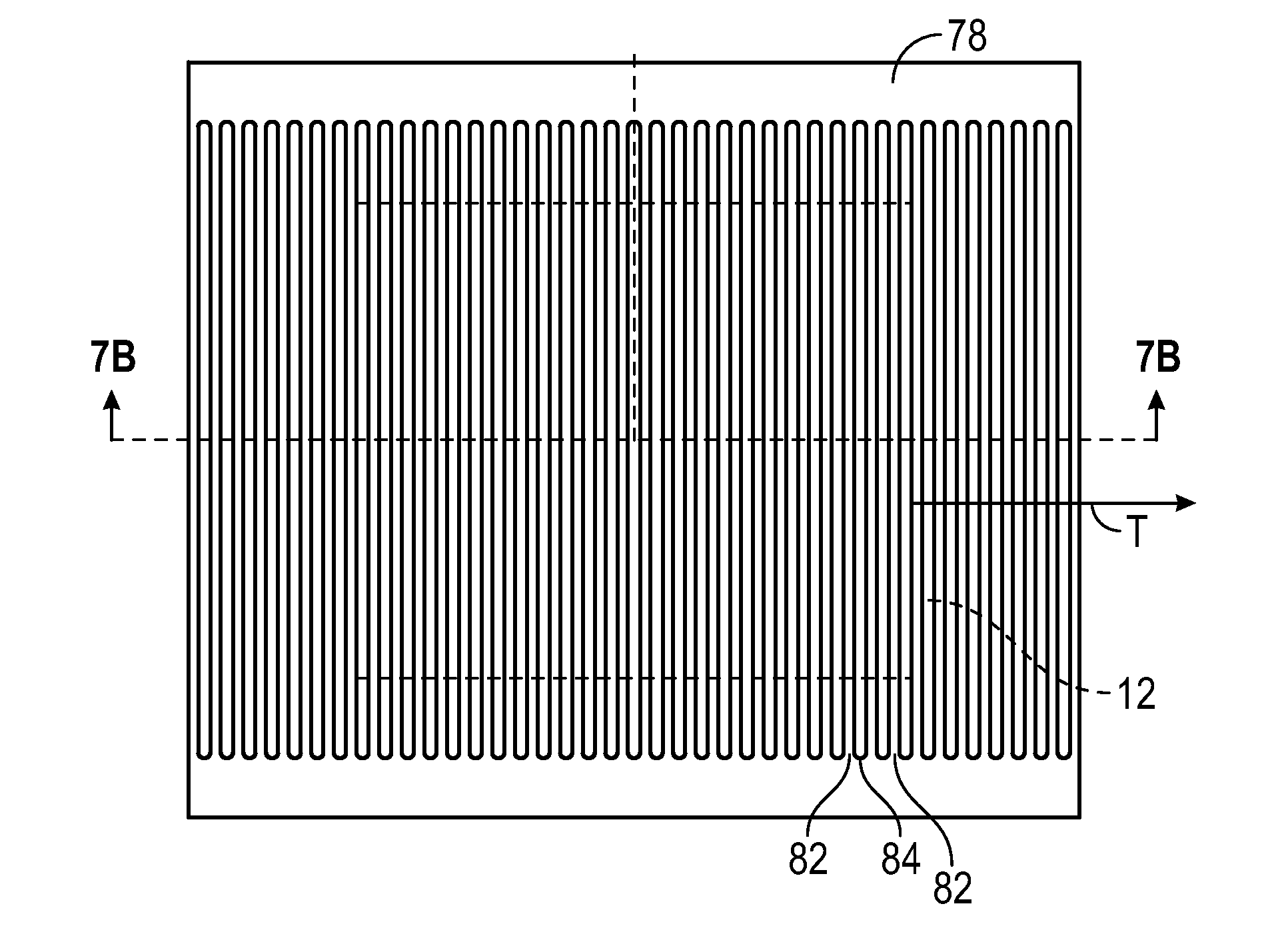
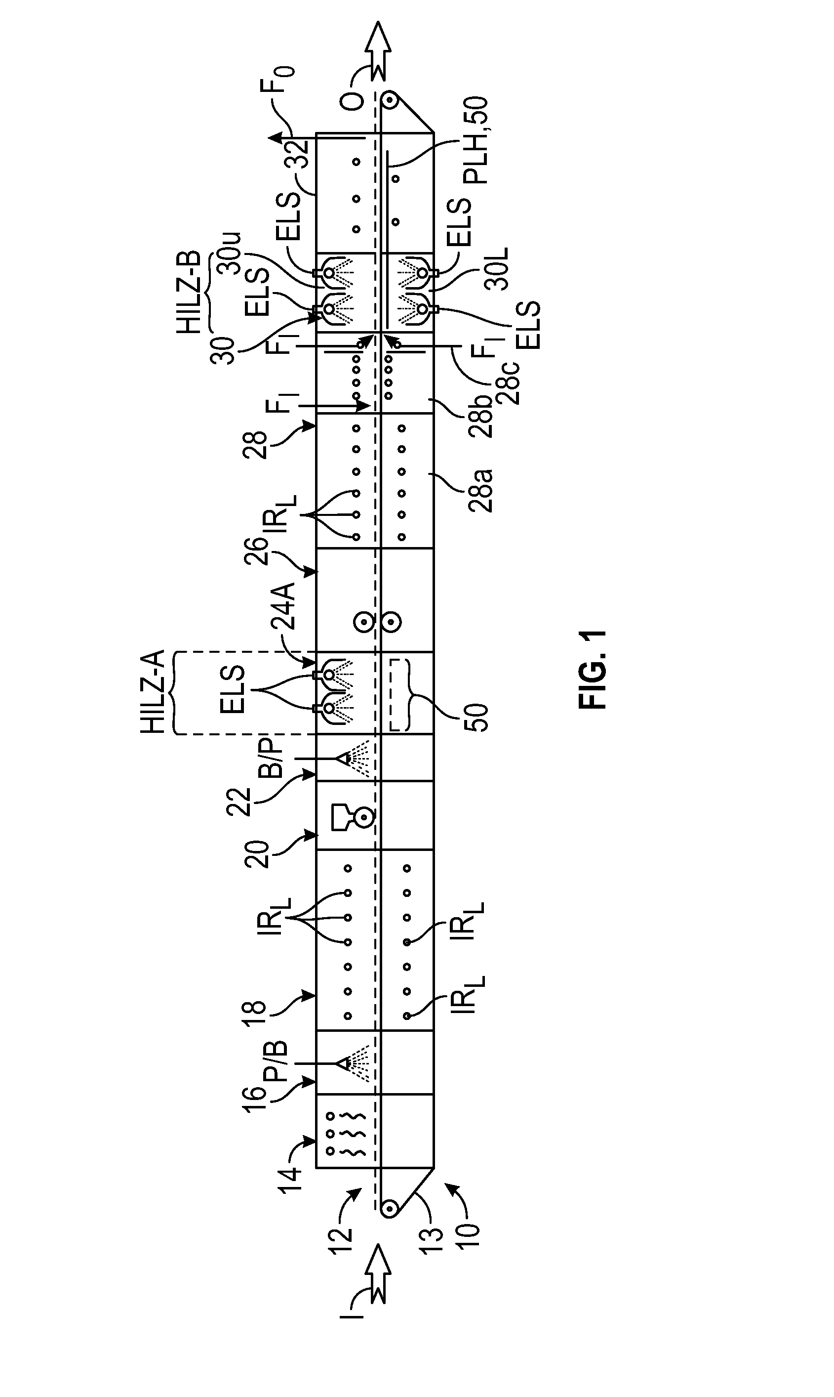
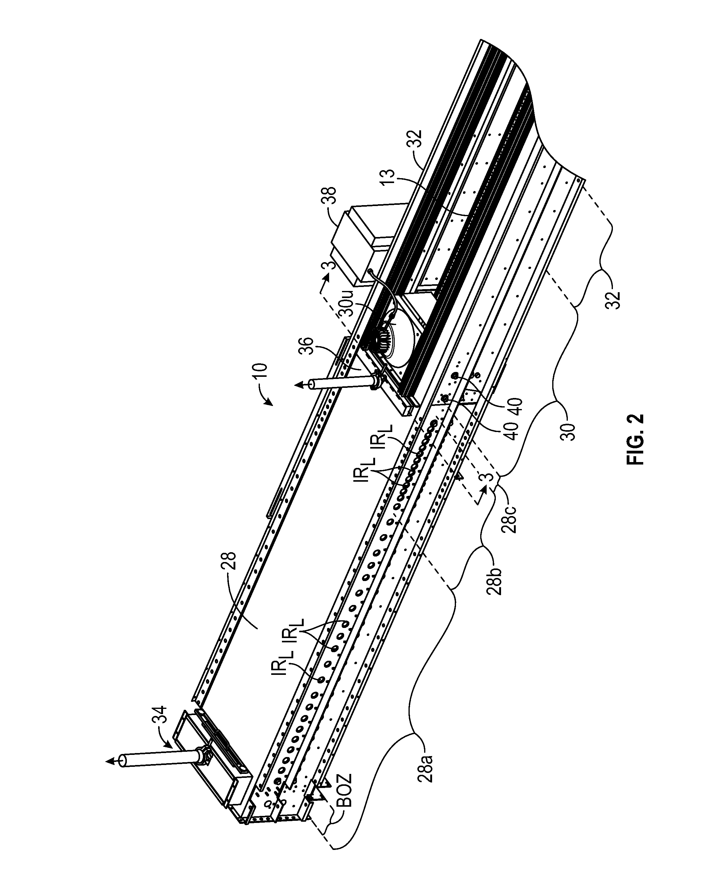
[0041]FIG. 1 shows a s...


PUM

PropertyMeasurementUnit
temperatureaaaaaaaaaa
temperaturesaaaaaaaaaa
sizeaaaaaaaaaa

Abstract

Reduction of solar wafer LID by exposure to continuous or intermittent High-Intensity full-spectrum Light Radiation, HILR, by an Enhanced Light Source, ELS, producing 3-10 Sols, optionally in the presence of forming gas or/and heating to within the range of from 100° C.-300° C. HILR is provided by ELS modules for stand-alone bulk/continuous processing, or integrated in wafer processing lines in a High-Intensity Light Zone, HILZ, downstream of a wafer firing furnace. A finger drive wafer transport provides continuous shadowless processing speeds of 200-400 inches/minute in the integrated furnace/HILZ. Wafer dwell time in the peak-firing zone is 1-2 seconds. Wafers are immediately cooled from peak firing temperature of 850° C.-1050° C. in a quench zone ahead of the HILZ-ELS modules. Dwell in the HILZ is from about 10 sec to 5 minutes, preferably 10-180 seconds. Intermittent HILR exposure is produced by electronic control, a mask, rotating slotted plate or moving belt.

Description

CROSS-REFERENCE TO RELATED CASE[0001]This is the Regular US patent application corresponding to, and claiming priority of, U.S. Provisional Application 62 / 065,441 filed Oct. 17, 2014 of the same inventors under the title Solar Cell Boron Passivation System, the benefit of the filing date of which is claimed under 35 USC §§119 and 120.FIELD[0002]The invention relates to apparatus and methods for processing solar cell wafers, and more particularly to systems for reduction of Light Induced Degradation, herein “LID”, either before or after metallization firing, by use of High-Intensity full-spectrum Light Radiation of heated wafer surface(s), herein “HILR”, to which Boron or a Boron-containing compound or component has been applied (also known as passivating Boron applied to at least one surface of a wafer). The HILR treatment of the wafer surface may be done in a High-Intensity Light Zone, herein HILZ”, in ambient atmosphere, or preferably in a controlled atmosphere, such as a forming ...

Claims


Application Information

Patent Timeline
Patent Type & Authority Applications(United States)
IPC IPC(8): H01L31/18H05B3/00H01L21/677H01L31/028H01L21/67
CPCH01L31/186H01L31/028H05B3/0047H01L21/67115H01L21/677H01L31/1864H01L21/263H01L31/1804H01L31/1876H01L21/67173H01L21/6776Y02E10/547H01J65/04H01L31/0288H01L31/1868H05B1/0233
Inventor REY-GARCIA, LUIS ALEJANDRORAGAY, PETER G.
Owner TP SOLAR OF USA
Why Eureka
Try Eureka