

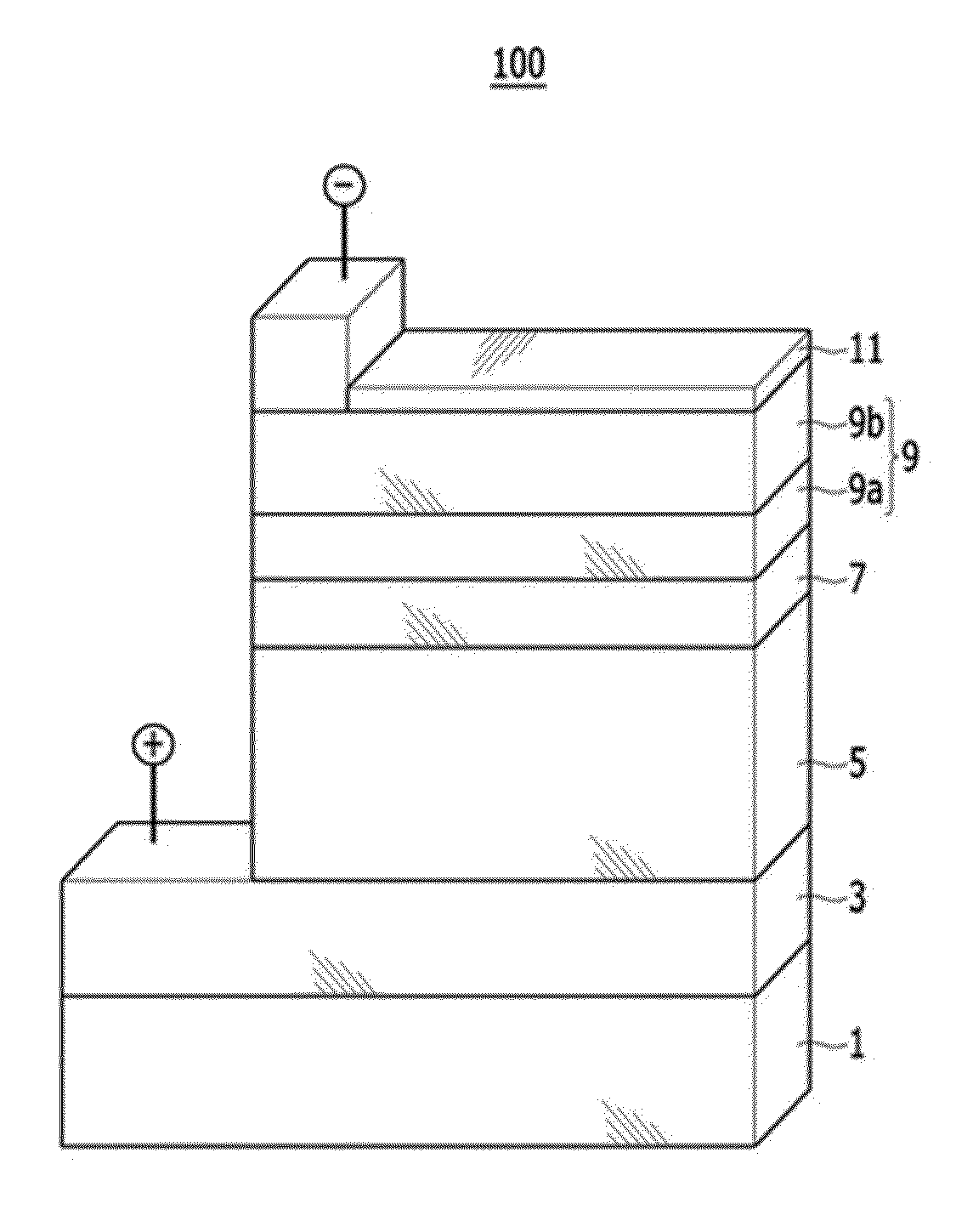
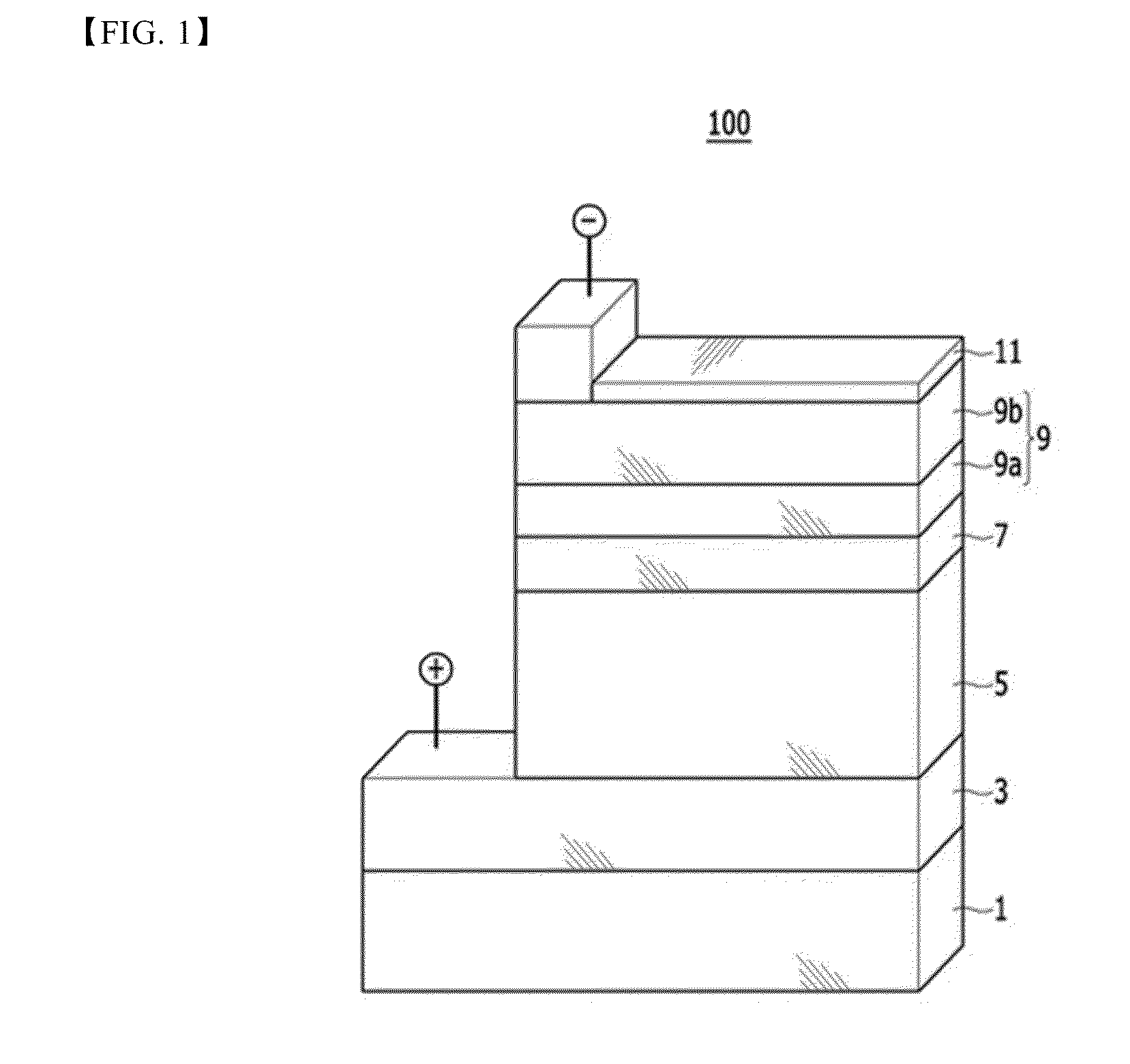
Solar cell and method for manufacturing same
a solar cell and manufacturing method technology, applied in the field of solar cells, can solve the problems that the wet cbd preparation method has been an obstacle to the vacuum inline process, and achieve the effects of improving the alignment properties of energy bands, excellent chemical resistance, and excellent reliability of thin films
- Summary
- Abstract
- Description
- Claims
- Application Information
AI Technical Summary
Benefits of technology
Problems solved by technology
Method used
Image

Examples
example 1
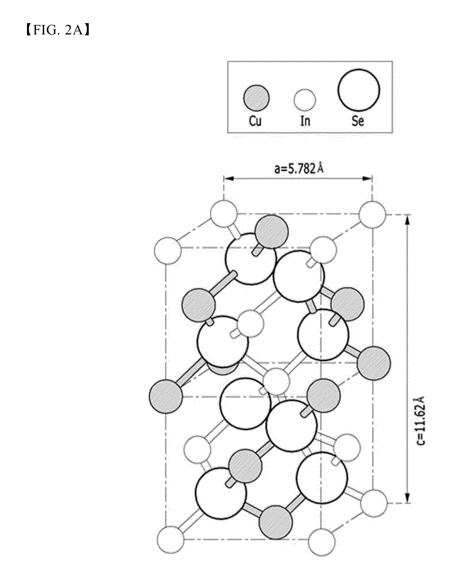
[0054]A buffer layer was formed on a light-absorbing layer formed of a CIGS-based semiconductor, Cu(In,Ga)Se2, by an atomic layer deposition process using tetrakis(dimethylamino)titanium (TDMAT) as a Ti precursor material.
[0055]The atomic layer deposition process was performed using a reactor with a scintillator precursor material inlet, a Ti precursor material inlet, and an oxygen gas inlet, and was performed in 4 steps.
[0056]In the atomic layer deposition process, a scintillator precursor material and atmospheric conditions are illustrated in FIG. 4. In FIG. 4, 2 s , 15 s, 4 s, and 15 s in the X-axis respectively denote implementation times in a first step, a second step, a third step, and a 4th step, a Ti precursor material and second Ar in the Y-axis represent materials injected into the scintillator precursor material inlet, and O2 and fourth Ar represent materials injected into the oxygen inlet.
[0057]As the conditions illustrated in FIG. 4, Ar gas, as a diluent gas, was inject...
example 2
[0065]A soda-lime glass substrate, a Mo back electrode disposed on the substrate, and a Cu(In,Ga)Se2, as a CIGS-based semiconductor, light-absorbing layer were sequentially formed. Subsequently, a buffer layer was formed on the light-absorbing layer by an atomic layer deposition process using tetrakis(dimethylamino)titanium (TDMAT) as a Ti precursor material.
[0066]The atomic layer deposition process was performed using a reactor with a scintillator precursor material inlet, a Ti precursor material inlet, and an oxygen gas inlet, and was performed in 4 steps.
[0067]In the atomic layer deposition process, a scintillator precursor material and atmospheric conditions are illustrated in FIG. 5. In FIG. 5, 1 s, 10 s, 4 s, and 5 s in the X-axis respectively denote implementation times in a first step, a second step, a third step, and a fourth step, a Ti precursor material and second Ar in the Y-axis represent materials injected into the scintillator precursor material inlet, and O2 and four...
PUM
| Property | Measurement | Unit |
|---|---|---|
| thickness | aaaaa | aaaaa |
| thickness | aaaaa | aaaaa |
| thickness | aaaaa | aaaaa |
Abstract
Description
Claims
Application Information