Planar lightwave circuit active connector

a technology of active connectors and lightwave circuits, applied in multiplex communication, optical elements, instruments, etc., can solve the problems of complex optical line cards and transport systems, large, and inconvenient assembly, and achieve the effect of simple and efficient, simple method of attaching the assembly

Active Publication Date: 2016-05-26
BROADEX TECH UK LTD
View PDF19 Cites 32 Cited by
  • Summary
  • Abstract
  • Description
  • Claims
  • Application Information

AI Technical Summary

Benefits of technology

[0010]Aspects of the invention provide a simple and efficient method of coupling light in and out of silicon photonics chips using a PLC as an intermediate material. By fabricating waveguide multiplexers and demultiplexers in glass PLCs, multi-wavelength fibers are broken down to individual wavelengths before entering or exiting the silicon and so each grating coupler in the silicon can be used only at a single wavelength, compensating for the limited optical bandwidth of the silicon grating couplers. Furthermore, using MEMS to couple lasers into a PLC can be used in the same PLC to provide the different wavelength laser sources for the silicon modulators. Some embodiments include structure discussed combining all three functions (Multiwavelength in for the receiver, multisources in as inputs for the modulators, and multiwavelengths out) on a single PLC and provides for a simple method of attaching the assembly to a silicon photonics chip.

Problems solved by technology

In the past few decades, the speed of electronic processing, powered by increasing levels of integrations and smaller gate geometries has overwhelmed the ability of these same silicon integrated circuits to transmit and receive the information that they process.
Thus the bottleneck in electronics is frequently the communication between chips, modules, or systems.
The optical line cards and transport systems are complex, large, and expensive, justified by the need for bandwidth efficiency in the very long links that they serve.
Perhaps the most significant issue with silicon photonics is that silicon as a material, unlike Indium Phosphide, does not possess a direct bandgap.
In a forward biased silicon pn junction, the carriers recombine non-radiatively and thus one cannot make LEDs or lasers in silicon.
The challenge here is of course the complexity of getting the light on and off the silicon chip, especially if multiple wavelengths or multiple sources of light are needed.
The different lattice constant, chemistry, and processing requirements of the indium phosphide make it difficult to fabricate efficient lasers this way.
Furthermore, it is impossible to test or burn-in the laser prior to assembly and the relatively poor yield of the lasers increases the cost of the entire assembly.
Needless to say, this is very challenging.
A second related issue with silicon photonics is the challenge of coupling light in and out of the chip.
The high contrast has the advantage of being able to make tight waveguide turns, the light paths almost having the geometries of electrical wires, but also has the disadvantage of being completely mismatched to a mode in a glass optical fiber, where the contrast is typically much less than 1% between the core and the cladding.
Grating couplers are frequently used to help with the alignment, but grating couplers generally work only at one wavelength and therefore limit the coupling to a single channel per port.
However, there are many penalties with this approach.
First it is difficult to cool the transceivers in the front panel.
A second issue is that high speed signals have to travel from a switch chip, somewhere on the board, all the way to the front panel.

Method used


Image

  • Planar lightwave circuit active connector
  • Planar lightwave circuit active connector
  • Planar lightwave circuit active connector

Examples


Embodiment Construction

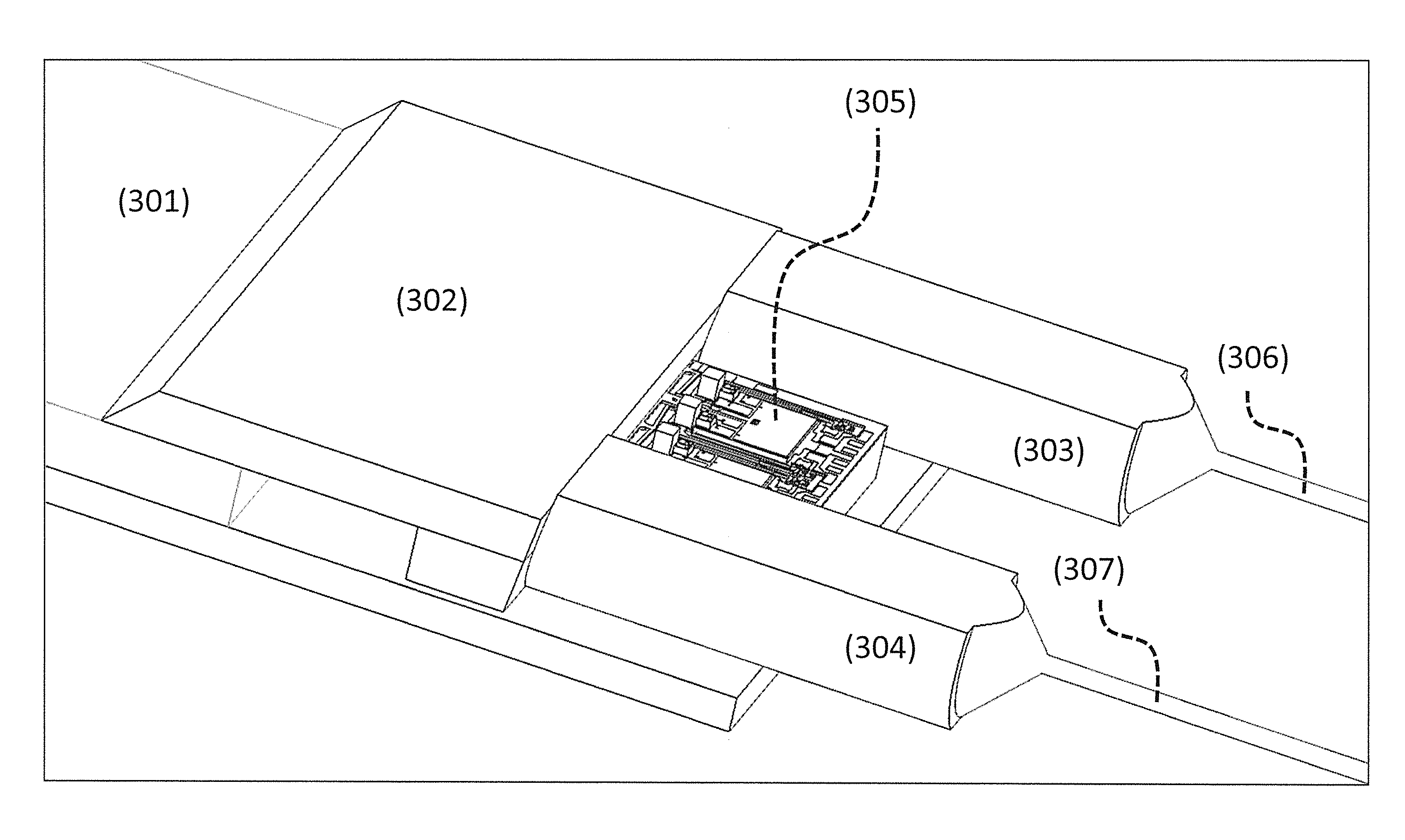
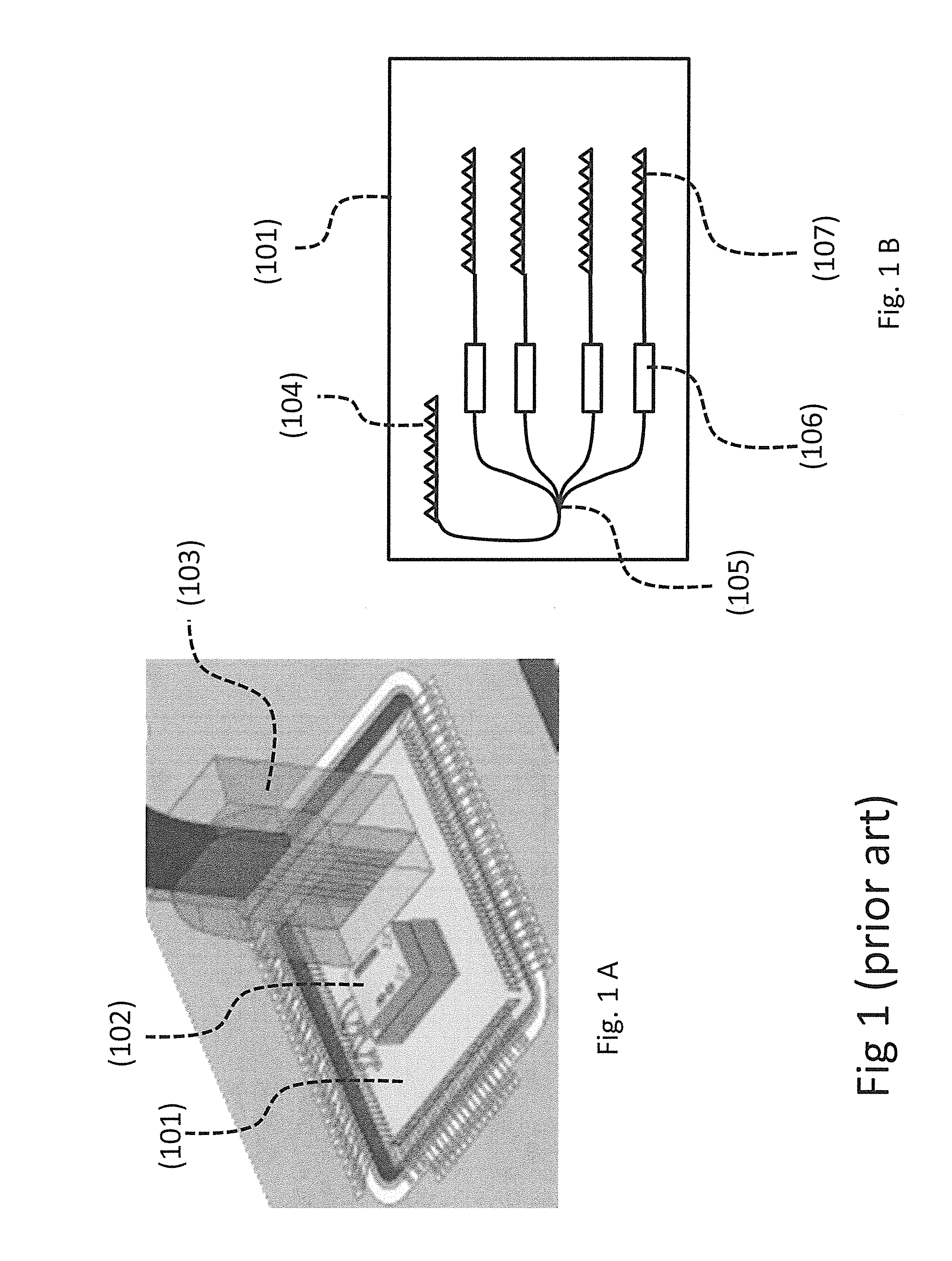
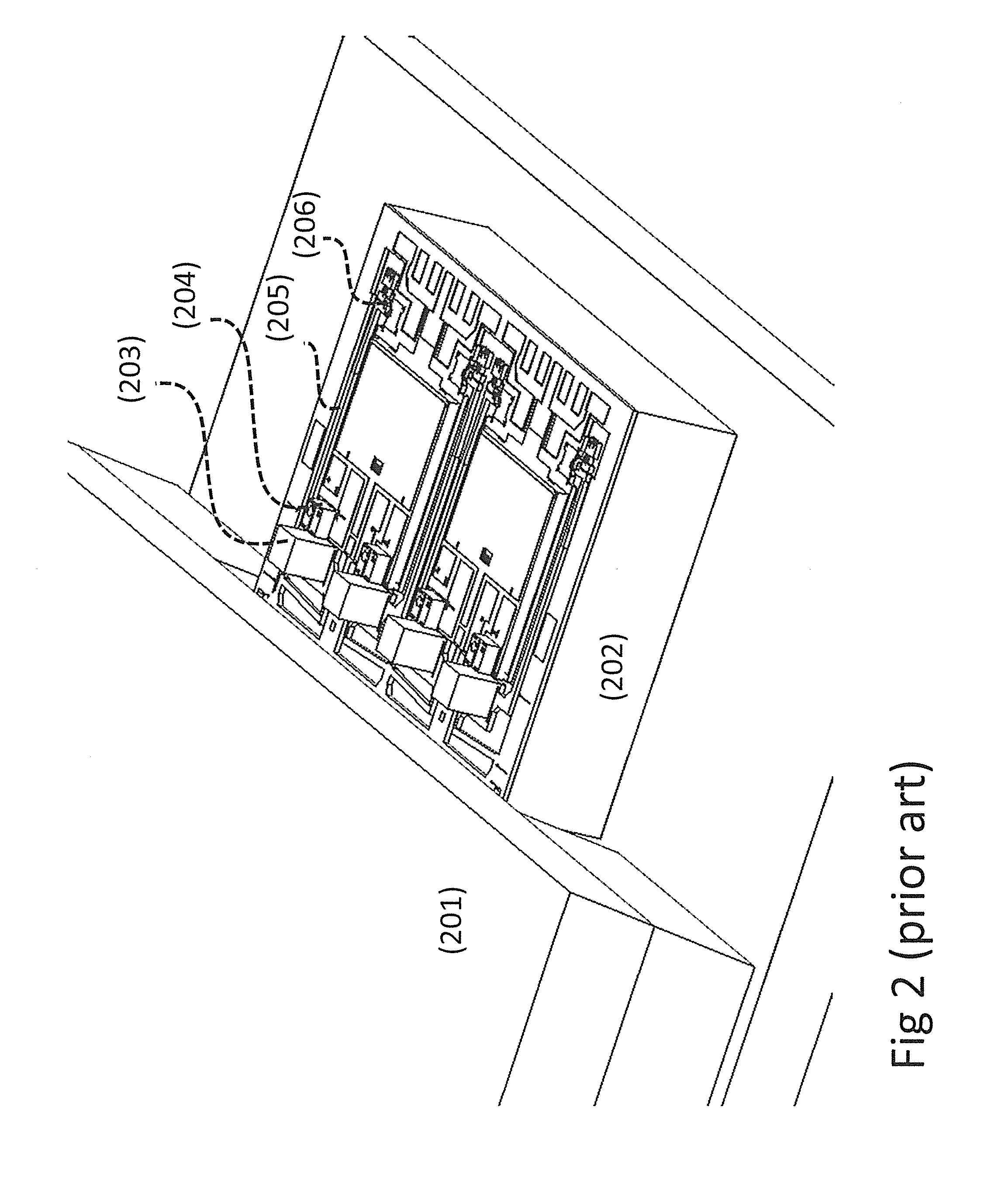
[0032]Silicon modulators are readily fabricated using standard processes in foundries and therefore can be used to generate modulated signals that can transmit information between electronic modules. As mentioned previously, it is extremely difficult to generate light in silicon, and therefore a separate light source, for example a laser, is generally needed that provides light coupled into the silicon photonics chip with the modulators. Similarly, the modulated light is coupled out of the chip and into fiber(s) to transmit the information. One way of coupling light in and out of very tight silicon waveguides is with a grating coupler, which can only operate efficiently at one wavelength. Given these limitations of standard silicon photonics, often a single high power external laser is used as the source for multiple modulators. As input coupling into the waveguides is challenging, coupling a single laser is simpler than coupling multiple lasers. This means that for multiple lanes, ...


PUM


Abstract

An assembly of waveguide wavelength multiplexers and demultiplexers, together with continuous wave (CW) laser transmitters that interface to grating couplers on a silicon photonics chip, providing CW sources, multiplexed output and optionally multiplexed input, all using a single photonic lightwave circuit (PLC).

Description

CROSS REFERENCE TO RELATED APPLICATIONS[0001]This application claims the benefit of the filing date of U.S. Provisional Patent Application No. 62 / 082,529, filed on Nov. 20, 2014, the disclosure of which is incorporated by reference herein.BACKGROUND OF THE INVENTION[0002]The present application relates generally to fiber optic communications and, more particularly, to optical communications using silicon photonic chips having optical modulators using silicon interfaced with passive planar lightwave circuits.[0003]In the past few decades, the speed of electronic processing, powered by increasing levels of integrations and smaller gate geometries has overwhelmed the ability of these same silicon integrated circuits to transmit and receive the information that they process. More and more electrical power and chip real-estate is devoted to driving the higher capacitance lines that carry signals off the integrated circuits. Thus the bottleneck in electronics is frequently the communicati...

Claims


Application Information

Patent Timeline
Patent Type & Authority Applications(United States)
IPC IPC(8): H04J14/02G02B6/122H04Q11/00G02B6/124G02B6/34G02B6/12G02B6/293
CPCH04J14/0212G02B6/12021G02B6/1228G02B6/2938G02B6/124G02B6/29329H04Q2011/0032H04Q11/0005G02B2006/12061G02B2006/12038G02B2006/12142H04Q2011/0016G02B6/34G02B6/30G02B6/4215G02B6/1223
Inventor SOLDANO, LUCASPEZESHKI, BARDIAHEANUE, JOHN
Owner BROADEX TECH UK LTD
Why Eureka
Try Eureka