Spectroscopic Beam Profile Metrology

a beam profile and metrology technology, applied in the field of spectroscopic beam profile metrology, can solve the problems of limiting the throughput of such systems, and presenting challenges in metrology applications involving the measurement of structures generated by semiconductor fabrication processes, so as to reduce coherence effects, improve accuracy, and improve measurement sensitivity

Active Publication Date: 2016-06-09
KLA TENCOR TECH CORP
View PDF2 Cites 48 Cited by
  • Summary
  • Abstract
  • Description
  • Claims
  • Application Information

AI Technical Summary

Benefits of technology

[0015]In another further aspect, a beam shaping optic is located in the illumination path. The beam shaping optic is configured to rotate the narrow line beam illumination to a desired azimuth angle. By rotating the narrow line beam illumination about the beam axis, the effective azimuth angle is changed. For some two dimensional measurement targets, such as a CD line-space grating, and some three dimensional measurement targets, such as a complex fin structure, measurement sensitivit...

Problems solved by technology

This limits the throughput of such systems when multiple illumination wavelengths are needed to accurately characterize the sample.
This limits the throughput of such system when multiple AOIs are required to accurately characterize the sample.
Metrology applications...

Method used


Image

  • Spectroscopic Beam Profile Metrology
  • Spectroscopic Beam Profile Metrology
  • Spectroscopic Beam Profile Metrology

Examples


Embodiment Construction

[0040]Reference will now be made in detail to background examples and some embodiments of the invention, examples of which are illustrated in the accompanying drawings.

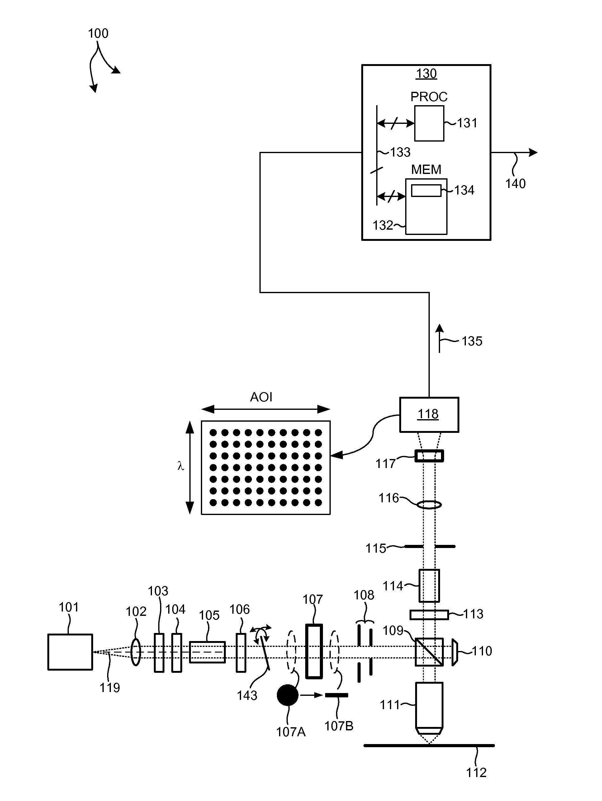
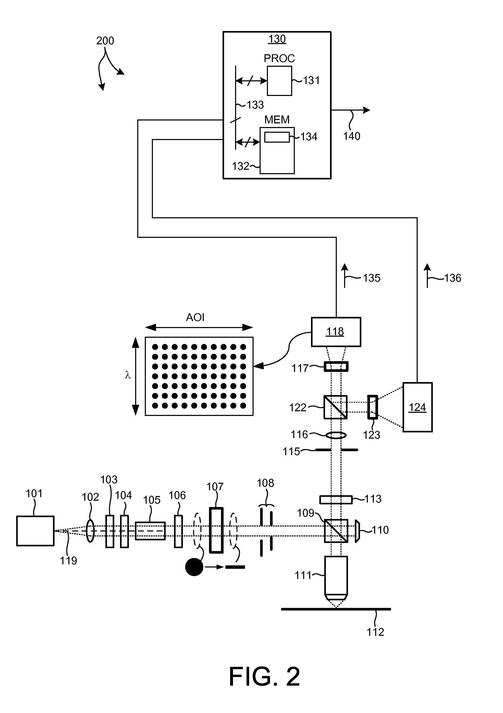
[0041]Methods and systems for broadband illumination and simultaneous detection of collected light over a broad range of angles of incidence and a broad range of wavelengths are presented herein. Several embodiments of a spectroscopic beam profile metrology system are presented herein for illustration purposes. In these embodiments, measurement signals over a large wavelength range and a large range of angle of incidence are simultaneously detected and spectroscopic beam profile metrology signals generated by the detection subsystem are generated within a short integration time.

[0042]In one aspect, a spectroscopic beam profile metrology system includes a light source that emits a collimated beam of light with multiple wavelengths. Beam shaping optics reshape the collimated beam of light to a narrow line beam of light ...


PUM


Abstract

A spectroscopic beam profile metrology system simultaneously detects measurement signals over a large wavelength range and a large range of angles of incidence (AOI). In one aspect, a multiple wavelength illumination beam is reshaped to a narrow line shaped beam of light before projection onto a specimen by a high numerical aperture objective. After interaction with the specimen, the collected light is passes through a wavelength dispersive element that projects the range of AOIs along one direction and wavelength components along another direction of a two-dimensional detector. Thus, the measurement signals detected at each pixel of the detector each represent a scatterometry signal for a particular AOI and a particular wavelength. In another aspect, a hyperspectral detector is employed to simultaneously detect measurement signals over a large wavelength range, range of AOIs, and range of azimuth angles.

Description

CROSS REFERENCE TO RELATED APPLICATION[0001]The present application for patent claims priority under 35 U.S.C. §119 from U.S. provisional patent application Ser. No. 62 / 088,290, entitled “Method and Apparatus of Measuring a Property of a Substrate,” filed Dec. 5, 2014, the subject matter of which is incorporated herein by reference in its entirety.TECHNICAL FIELD[0002]The described embodiments relate to metrology systems and methods, and more particularly to methods and systems for improved measurement of parameters characterizing semiconductor manufacturing processes and structures generated by semiconductor manufacturing processes.BACKGROUND INFORMATION[0003]Semiconductor devices such as logic and memory devices are typically fabricated by a sequence of processing steps applied to a specimen. The various features and multiple structural levels of the semiconductor devices are formed by these processing steps. For example, lithography among others is one semiconductor fabrication p...

Claims


Application Information

Patent Timeline
IPC IPC(8): G01B11/00G03F7/00
CPCG03F7/00G01B11/002G01B11/24G01N21/956G01N2021/213G01B2210/56
Inventor FU, JIYOUSAPIENS, NOAMPETERLINZ, KEVIN A.PANDEV, STILIAN IVANOV
Owner KLA TENCOR TECH CORP
Why Eureka
Try Eureka