

Copper wiring forming method, film forming system, and storage medium
a technology of copper wiring and film forming, applied in the direction of electrolysis components, coatings, vacuum evaporation coatings, etc., can solve the problem of difficult filling of cu holes, and achieve the effect of reducing the resistance and suppressing the increase of via resistan
- Summary
- Abstract
- Description
- Claims
- Application Information
AI Technical Summary
Benefits of technology
Problems solved by technology
Method used
Image

Examples
Embodiment Construction
[0025]Hereinafter, an embodiment of the present invention will be described referring to the drawings.
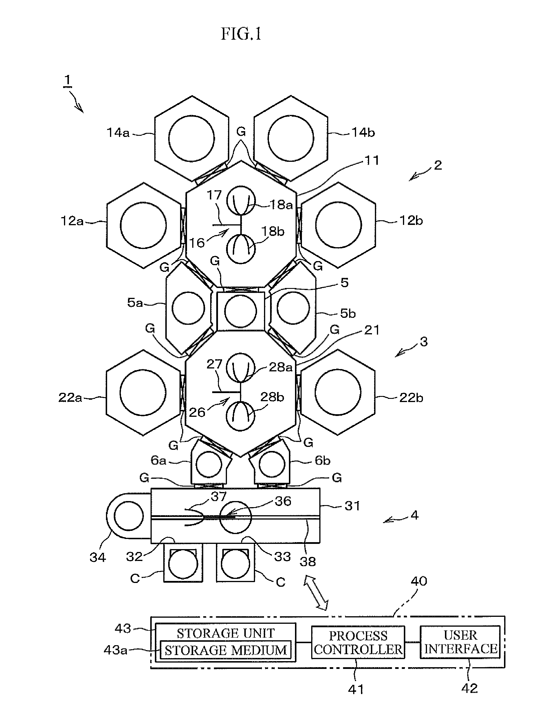
[0026]First of all, a film forming system used in the embodiment of the present invention will be described. FIG. 1 is a plan view illustrating an example of a multi-chamber film forming system for implementing formation of Cu wiring according to the embodiment of the present invention.
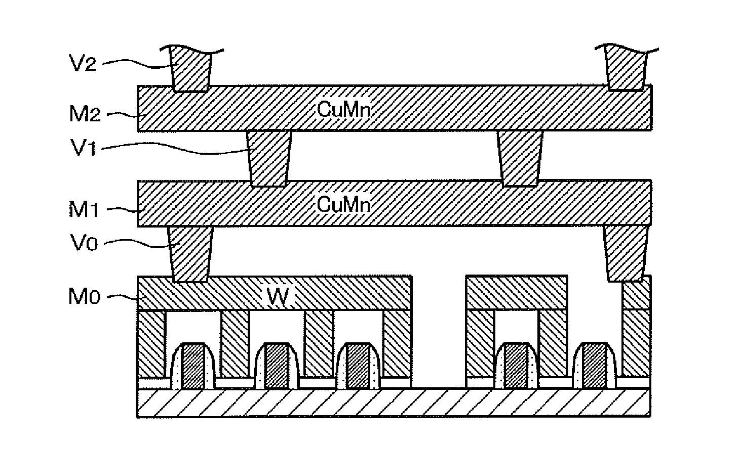
[0027]A film forming system 1 has: a first processing unit 2 that forms a nitriding preventing film, a barrier film, and a liner film; a second processing unit 3 that forms a Cu film; and a transfer-in / out unit 4, and is for forming Cu wiring on a semiconductor wafer (hereinafter, simply mentioned as a wafer) F.
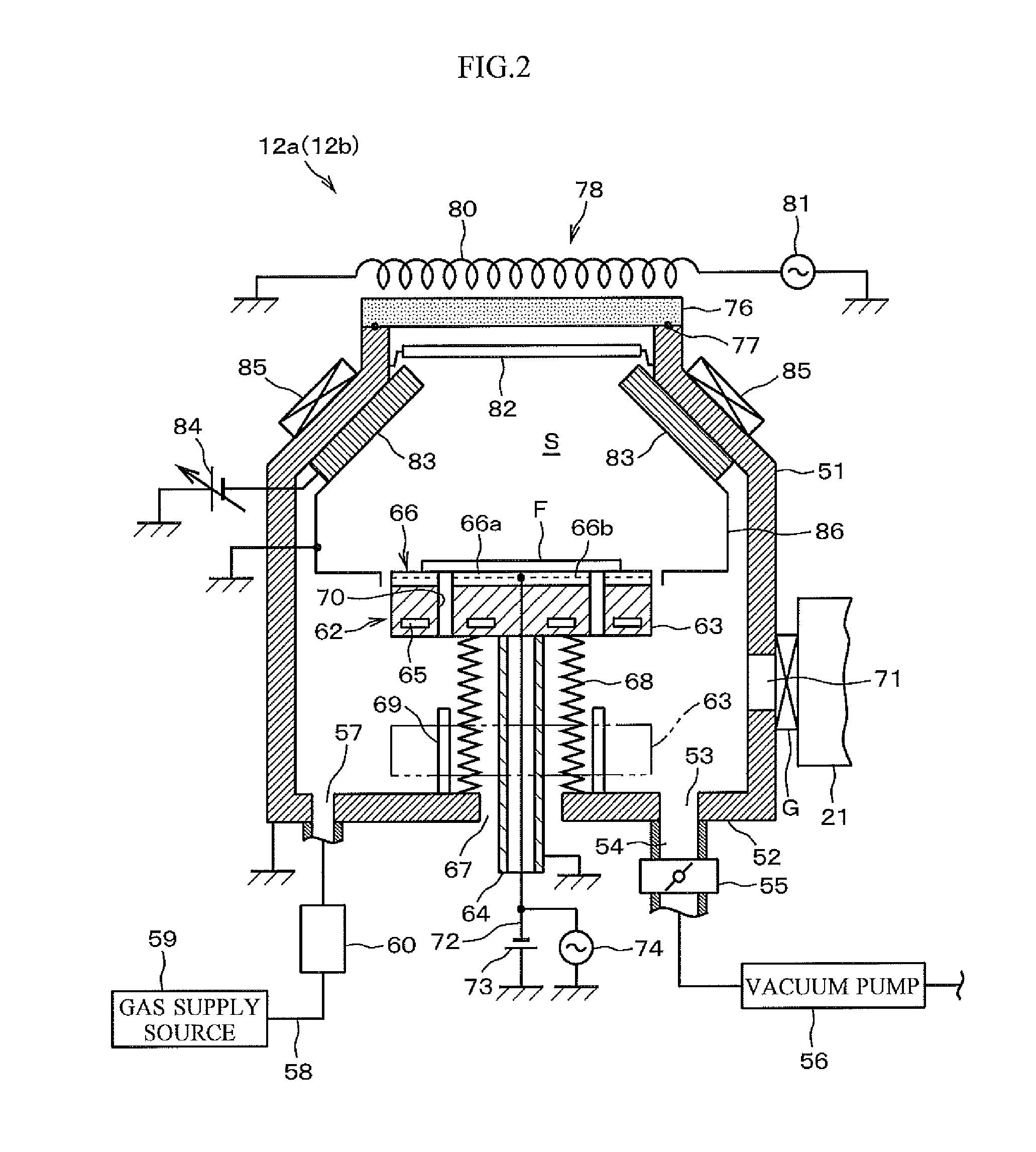
[0028]The first processing unit 2 has a first vacuum transfer chamber 11 having a planar shape forming a heptagon, and two nitriding preventing film and barrier film forming apparatuses 12a, 12b and two liner film forming apparatuses 14a, 14b, which are connected to wall portions corresponding ...
PUM
| Property | Measurement | Unit |
|---|---|---|
| thickness | aaaaa | aaaaa |
| temperature | aaaaa | aaaaa |
| frequency | aaaaa | aaaaa |
Abstract
Description
Claims
Application Information