Laminate and application therefor

Inactive Publication Date: 2016-06-16
FUJIFILM CORP
View PDF0 Cites 8 Cited by
  • Summary
  • Abstract
  • Description
  • Claims
  • Application Information

AI Technical Summary

Benefits of technology

The present invention provides a laminate that can temporarily support a member to be treated with strong adhesive force and can easily release the temporary support without damaging the treated member even after undergoing a process at a high temperature in a vacuum. The laminate includes an adhesive layer, a protective layer, and a device wafer in this order. The adhesive layer is a cured product of an adhesive layer precursor that includes a polymerizable compound. The laminate has both excellent adhesiveness during the formation of a thinner wafer and peelability after the formation of the thinner wafer. The laminate also has excellent properties after a high-temperature process, such as easy release without damaging the treated member and improved total thickness variation of the device wafer. A composition for forming a protective layer, a composition for forming an adhesive layer, and a kit for using the laminate are also provided.

Problems solved by technology

Therefore, in the case where the whole device surface of the semiconductor wafer and the support substrate are temporarily adhered to each other through the adhesive layer, when the temporary adhesion between the semiconductor wafer and the support substrate is made sufficient in order to support the semiconductor wafer stably and while not damaging the semiconductor wafer, due to too strong temporary adhesion between the semiconductor wafer and the support substrate, on the other hand, a problem in that the device is damaged or in that the device is dissociated from the semiconductor wafer is likely to occur, when the semiconductor wafer is dissociated from the support substrate.
Furthermore, the method of forming as a separation layer, a plasma polymer layer by a plasma deposition method between the wafer and the support layer system as in JP2009-528688A in order to prevent the adhesion between the wafer and the support layer system becoming too strong has problems (1) in that the equipment cost for performing the plasma deposition method is ordinarily high; (2) in that the layer formation by the plasma deposition method requires time for vacuumization in the plasma apparatus and deposition of monomers; (3) in that even when the separation layer formed of a plasma polymer layer is provided, it is not easy to control the adhesive bond in such a manner that the wafer is easily dissociated from the separation layer in the case of releasing the supporting of the wafer, while, on the other hand, the adhesive bond between the wafer and the separation layer is sufficiently maintained in the ease of supporting the wafer subjected to the processing; and in others.
Moreover, in a method of releasing the temporary adhesion with heating as described in JP2011-225814A, JP2011-052142A, JP2010-506406A, and US2012 / 0034437A, a problem in that the device may be damaged when the semiconductor wafer is dissociated is likely to occur.

Method used


Image

  • Laminate and application therefor
  • Laminate and application therefor
  • Laminate and application therefor

Examples


examples

[0509]The present invention will be described more specifically with reference to Examples, but the present invention is not limited thereto as long as the gist of the present invention is not deviated. Here, “part(s)” and “%” are on the basis of mass unless otherwise specified.

[0510]

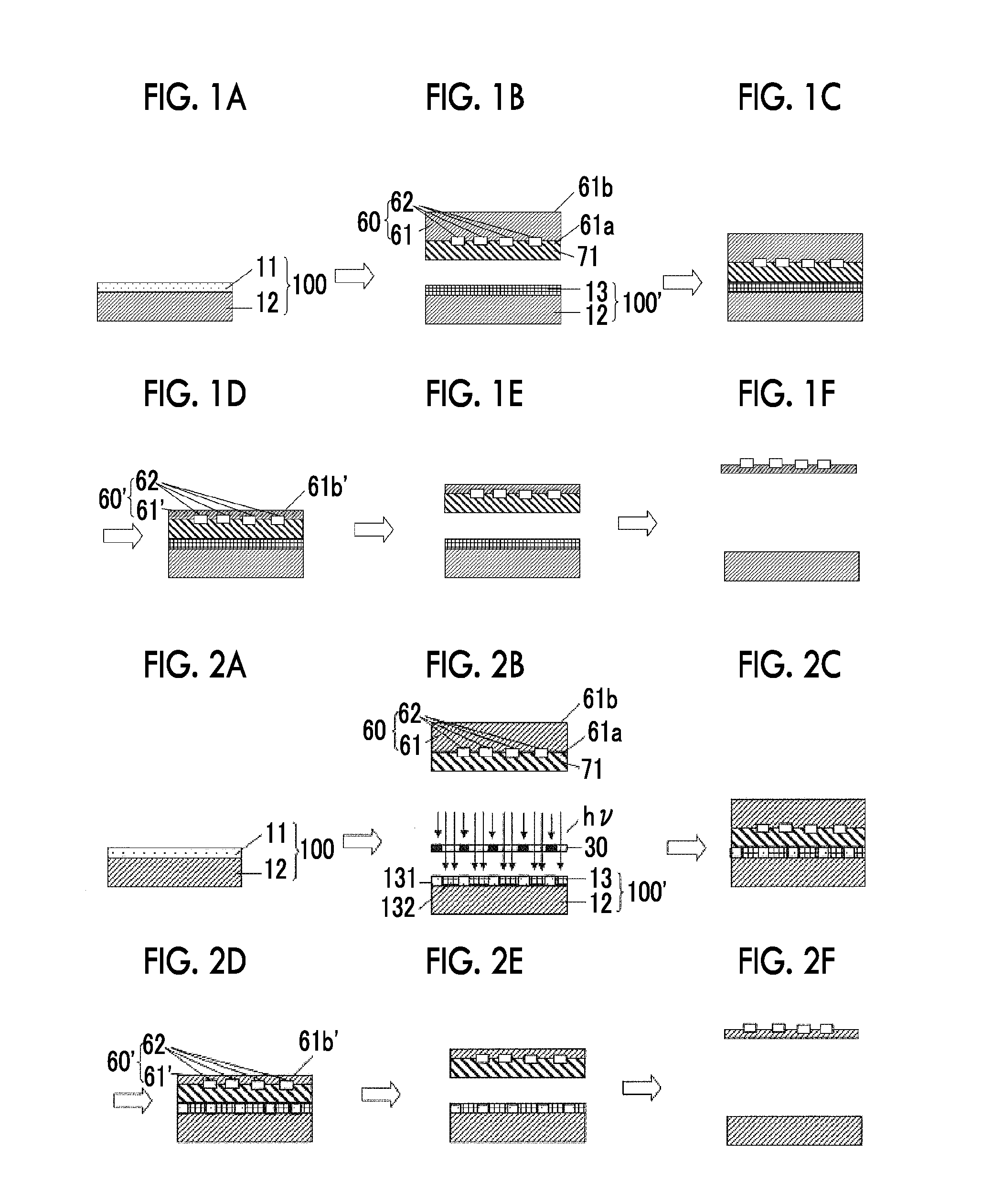
[0511]The adhesive layer precursor (composition for forming an adhesive layer) as described below was coated on a 200-mm Si wafer by a spin coater and then baked at 120° C. for 30 seconds to form a wafer having provided thereon an adhesive precursor having a thickness of 0.2 μm. Thereafter, light irradiation was carried out by using a mask (area ratio of the light-shielding area: 3%) so as to form a halftone dot region as in FIG. 4 using light at a wavelength of 365 nm, by means of a heating or UV Exposure Apparatus (LC8 manufactured by Hamamatsu Photonics K. K.) using a hot plate under the polymerization conditions shown in the following table (bake conditions or exposure doses), thereby forming a supp...


PUM

PropertyMeasurementUnit
Temperatureaaaaaaaaaa

Abstract

Provided are a laminate capable of providing a temporary support for a member to be treated by a strongly adhesive force when the member to be treated is subjected to a mechanical or chemical treatment, and of easily releasing the temporary support for the treated member while not damaging the treated member, in which the TTV of the treated member is excellent; a composition for forming a protective layer; a composition for forming an adhesive layer; and a kit.The laminate has, on a support (A), an adhesive layer having a softening point of 250° C. or higher (B), a protective layer (C), and a device wafer (D) in this order, in which the adhesive layer (B) is a cured product of an adhesive layer precursor and the adhesive layer precursor has a polymerizable compound (b-1).

Description

[0001]This application is a Continuation of PCT International Application No. PCT / JP2014 / 072368 filed on Aug. 27 2014, which claims priority under 35 U.S.C §119(a) to Japanese Patent Application No. 2013-180041 filed on Aug. 30, 2013. Each of the above application(s) is hereby expressly incorporated by reference, in its entirety, into the present application.BACKGROUND OF THE INVENTION[0002]1. Field of the Invention[0003]The present invention relates to a laminate, a composition for forming a protective layer, a composition for forming an adhesive layer, and a kit. More specifically, the present invention relates to a laminate temporarily bonded to a support using a temporary adhesive for producing a semiconductor device; a composition for forming a protective layer and a composition for forming an adhesive layer, each of which is used in the laminate; and a kit including the composition for forming a protective layer and the composition for forming an adhesive layer.[0004]2. Descri...

Claims


Application Information

Patent Timeline
IPC IPC(8): C09J4/06C09D169/00H01L21/683C09D145/00C09J4/00C09D181/06C09D125/06
CPCC09J4/06C09D181/06C09D169/00C09D125/06H01L2221/6834C09J4/00H01L21/6835H01L2221/68318C09D145/00H01L2221/68327H01L2221/68381B32B7/12B32B27/06B32B27/281B32B27/288B32B27/36B32B3/08B32B2457/00B32B2457/14H01L2224/81H01L2224/95C08F222/1063C08F222/104C08F222/103C08F222/102C09J201/00
Inventor IWAI, YUKOYAMA, ICHIROKAMOCHI, YOSHITAKA
Owner FUJIFILM CORP
Why Eureka
Try Eureka