Methods of fabricating polygon-sectional rodlike ingot and substrate with orientation marker or rounded corners, rodlike ingot and substrate

a technology of orientation markers and substrates, applied in the field of polygonal sheet substrates, can solve the problems of reduced effective usage area, low identification ability of surface orientation markers, yield and production efficiency reduction, etc., and achieves easy and reliable implementation of identification and high identification ability.

Inactive Publication Date: 2016-07-14
INST OF SEMICONDUCTORS - CHINESE ACAD OF SCI
View PDF1 Cites 6 Cited by
  • Summary
  • Abstract
  • Description
  • Claims
  • Application Information

AI Technical Summary

Benefits of technology

[0010]An object of the present invention is to provide a quadrate-sectional or polygon-sectional rodlike ingot and a method of forming a surfa

Problems solved by technology

Placement of the circular substrate on the circular graphite susceptor will cause a reduced effective usage area.
However, when there is no large difference between lengths of the two cut sides, the mar

Method used


Image

  • Methods of fabricating polygon-sectional rodlike ingot and substrate with orientation marker or rounded corners, rodlike ingot and substrate
  • Methods of fabricating polygon-sectional rodlike ingot and substrate with orientation marker or rounded corners, rodlike ingot and substrate
  • Methods of fabricating polygon-sectional rodlike ingot and substrate with orientation marker or rounded corners, rodlike ingot and substrate

Examples


first embodiment

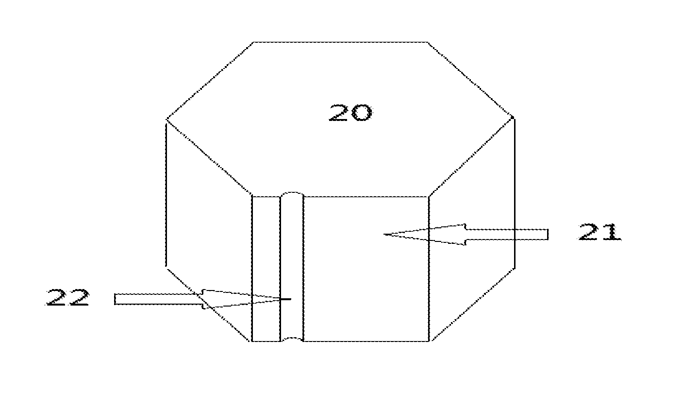
[0034]FIGS. 1-3 show quadrate-sectional or polygon-sectional rodlike ingots and a method of forming a surface orientation marker on the quadrate-sectional or polygon-sectional rodlike ingot, according to a The method includes: selecting, one of sides of the polygon-sectional rodlike ingot that is parallel to an axial direction axial direction of the rodlike ingot, as a first feature of the orientation marker; and forming a minisize notch, which is parallel to an edge of the rodlike ingot, in the one of sides as the first feature in the axial direction of the rodlike ingot, as a second feature of the orientation marker.

[0035]Specifically, the method comprises:

[0036]step 1: selecting a random cylinder surface of the polygon-sectional rodlike ingot 20 that is parallel to an axial direction thereof as a first feature 21 for the surface orientation marker, wherein the polygon-sectional rodlike ingot 20 may be made of sapphire, silicon carbide, gallium nitride, aluminum nitride, gallium ...

second embodiment

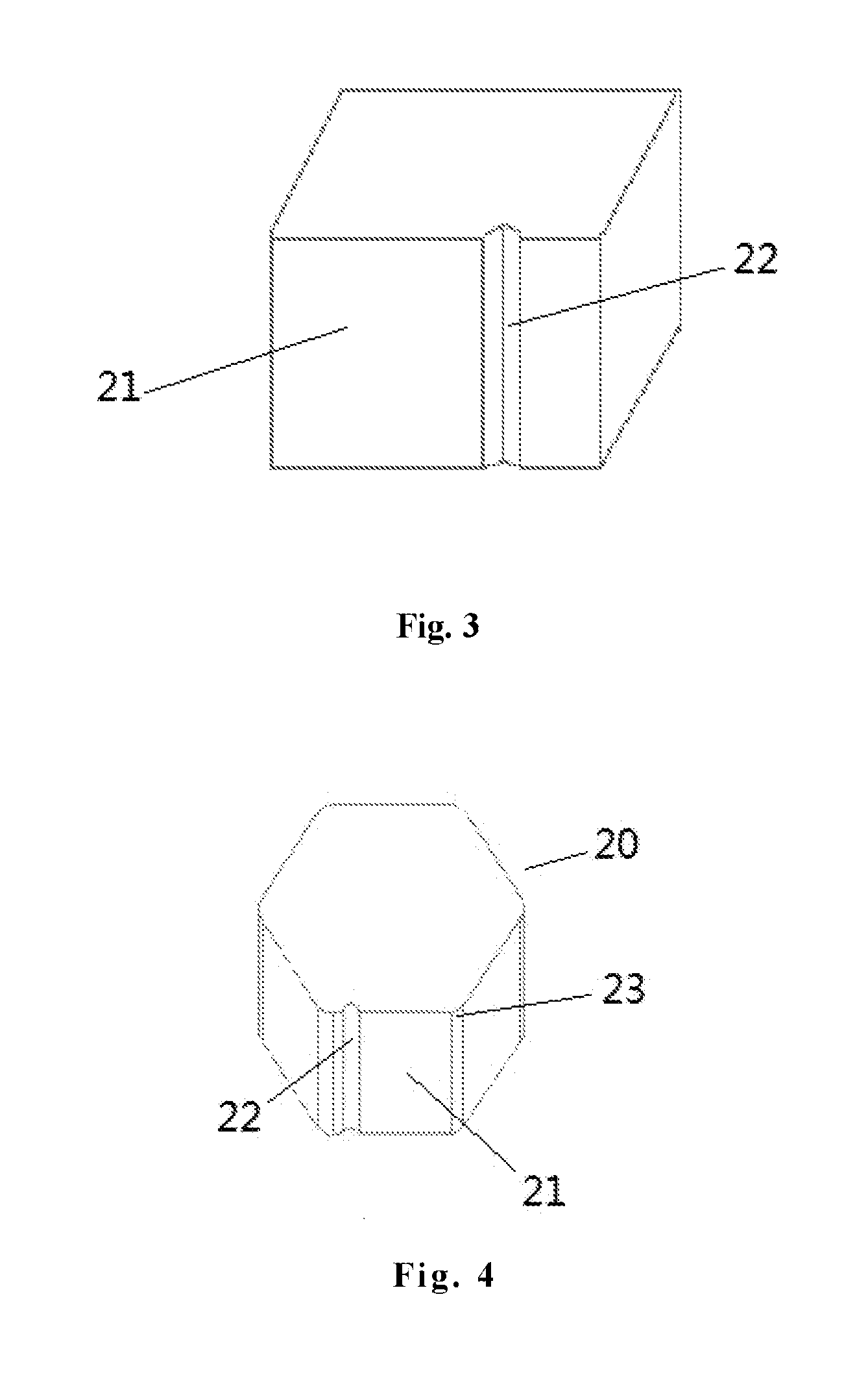
[0048]According to the present invention, a polygonal rodlike ingot 20 may be rounded at edges thereof, as shown in FIGS. 4 and 5, in order to increase yields of subsequent products such as a substrate, an epitaxial wafer and the like. The procedure is shown as below.

[0049]Firstly, edges of the polygonal rodlike ingot 20 are rounded, for example, may be ground by a surface-grinding machine or a shaping wheel to obtain an arc surface having a preset curvature radius or a plane with a preset width.

[0050]Subsequently, similar to the process of forming an orientation marker according to the first embodiment, one of sides 21 is selected as a first feature and a second feature 22 is formed on the one of sides 21. A combination of the first feature and the second feature form a marker for the polygonal rodlike ingot 20 and a subsequently formed substrate.

[0051]In an example, the polygonal rodlike ingot 20 may be made of sapphire, silicon carbide, gallium nitride, aluminum nitride, gallium ...

third embodiment

[0053]the present invention will be described hereinafter with reference to FIGS. 6-8. The existing chemical vapor deposition apparatus has a relative low yield and thus an epitaxial wafer is produced in relative high cost, which does not meet requirements of application. It is investigated and found by the inventor that, in a chemical vapor deposition apparatus in prior art, a substrate arranged in a graphite susceptor is designed in a circular shape, which renders a low availability ratio of the graphite susceptor and then a limited amount of substrates processed in one furnace of the chemical vapor deposition apparatus. As an example, a most common graphite susceptor that is used in K465i type MOCVD available from Veeco company and has a diameter of 45 cm may be filled by 45 circular substrates of 2 inches if no substrate is placed within the central region of the susceptor, only obtaining a surface availability ratio of 53.9% of the graphite susceptor; and, it may be filled by 5...


PUM


Abstract

The present invention discloses a method of forming a polygon-sectional rodlike ingot having an orientation marker or rounded corners, a rodlike ingot and a sheet substrate so formed. The method comprises: selecting one of sides of the polygon-sectional rodlike ingot that is parallel to an axial direction thereof as a first feature of a surface orientation marker; forming a minisize notch, which is parallel to an edge, in the one of sides selected as the first feature in the axial direction of the rodlike ingot, as a second feature of the orientation marker; and processing the rodlike ingot to form rounded corners. The sheet substrate is obtained by cutting the rodlike ingot.

Description

BACKGROUND[0001]1. Technical Field[0002]The present invention is related to semiconductor technology field, and particularly, to a polygonal sheet substrate used in process of fabricating a LED by metal organic chemical vapor deposition (MOCVD) equipment.[0003]2. Description of the Related Art[0004]The third-generation semiconductor materials represented by GaN and its alloys are new type of semiconductor materials which have obtained great interests in recent more than decade years. This type of semiconductor materials have lots of outstanding properties, such as a wide forbidden band, a high electron saturation drift speed, a small dielectric constant, a good thermal conduction, a stable structure and so on. Thus, nitride materials produce an excellent application prospect in the fields of optoelectronic and microelectronic technologies.[0005]The current method of fabricating GaN-based opto-electronic devices, such as LEDs, mainly relates to MOCVD epitaxial technology. Generally, ...

Claims


Application Information

Patent Timeline
IPC IPC(8): C30B25/18B28D5/04C30B29/16C30B29/66C30B29/64
CPCC30B25/18C30B29/66B28D5/04C30B29/16C30B29/64H01L22/20H01L2223/54493C30B25/00
Inventor LI, JINMINWANG, JUNXIYI, XIAOYANKONG, QINGFENGWANG, WENJUNHU, QIANGYAN, JIANCHANGWEI, TONGBOMA, PINGLU, HONGXIJI, PANFENGGUO, JINXIA
Owner INST OF SEMICONDUCTORS - CHINESE ACAD OF SCI
Why Eureka
Try Eureka