Trench lateral diffusion metal oxide semiconductor device and manufacturing method of the same

a metal oxide semiconductor and manufacturing method technology, applied in the field of semiconductor devices, can solve the problems of increasing manufacturing costs, complicating the manufacturing steps of trench ldmos transistors, and small distance between trench gate and source/drain region, so as to prevent leakage current

Inactive Publication Date: 2016-07-21
MAXCHIP ELECTRONICS CORP
View PDF0 Cites 17 Cited by
  • Summary
  • Abstract
  • Description
  • Claims
  • Application Information

AI Technical Summary

Benefits of technology

[0008]The invention provides a trench LDMOS device, a trench gate protrudes from a surface of the substrate, and electrical connection of the trench gate and a doped region due to metal silicide may be prevented, enhancing the performance of the device.
[0036]Furthermore, a trench gate protrudes from a surface of the substrate, and electrical connection of the trench gate and a doped region due to a metal silicide may be prevented.
[0037]In addition, the gate dielectric layer of the trench LDMOS transistor does not produce an electric field, therefore leakage current may be prevented.

Problems solved by technology

When forming openings of different depth, different manufacturing parameters are needed (for example, etching time or the like), as a result causing an increase in manufacturing costs and complicating the manufacturing steps of a trench LDMOS transistor.
Furthermore, a top portion of the trench gate is lower than the surface of the substrate, making the distance between the trench gate and source / drain regions small, and a short circuit will form between the trench gate and the source / drain regions due to the metal silicide manufacturing process.

Method used


Image

  • Trench lateral diffusion metal oxide semiconductor device and manufacturing method of the same
  • Trench lateral diffusion metal oxide semiconductor device and manufacturing method of the same
  • Trench lateral diffusion metal oxide semiconductor device and manufacturing method of the same

Examples


Embodiment Construction

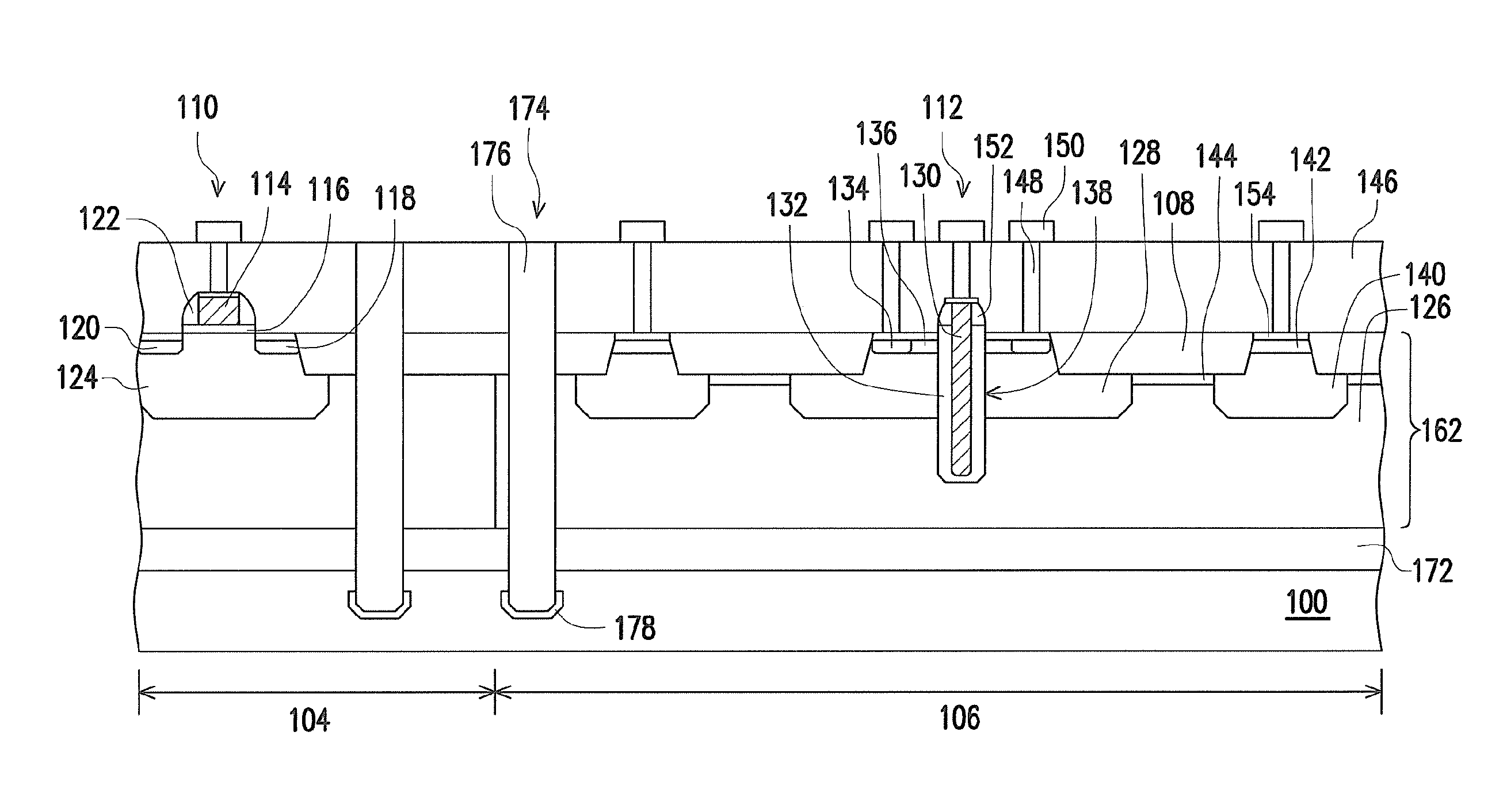
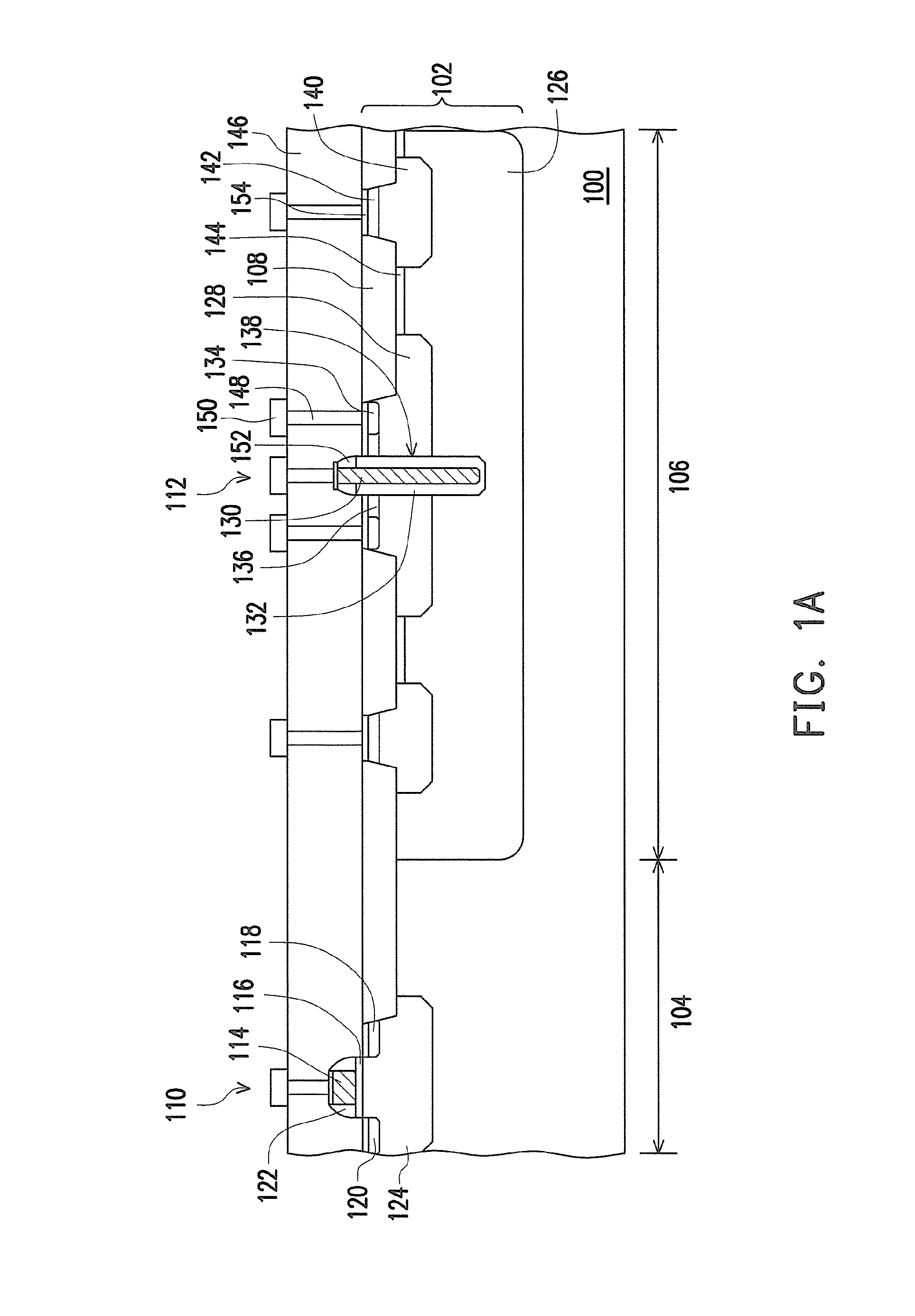
[0046]Reference will now be made in detail to the present preferred embodiments of the invention, examples of which are illustrated in the accompanying drawings. Wherever possible, the same reference numbers are used in the drawings and the description to refer to the same or like parts.

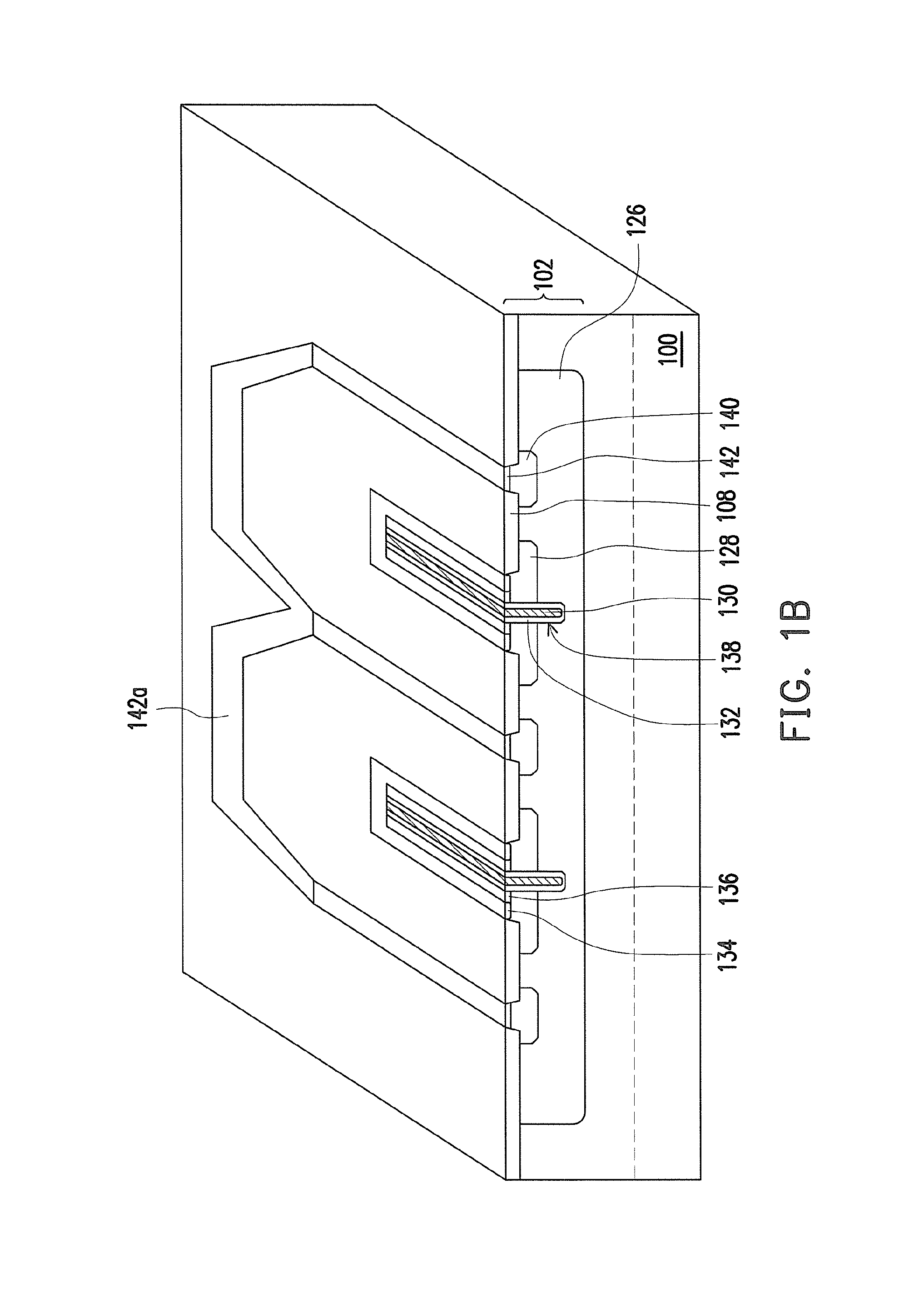
[0047]FIG. 1A is a cross-sectional view illustrating a trench LDMOS device according to an embodiment of the invention. FIG. 1B˜FIG. 1D are three dimensional structural schematics respectively illustrating a trench LDMOS device according to an embodiment of the invention. In FIG. 1B˜FIG. 1D, similar components with FIG. 1A are given the same reference numbers, and detailed description similar components will be omitted.

[0048]Referring to FIG. 1A, a trench LDMOS device is disposed on a substrate 100. The substrate 100 includes an epitaxial layer 102, and may be separated into a first area 104 and a second area 106, and an element isolation structure 108 formed in the substrate 100. The element isolati...


PUM


Abstract

A trench lateral diffusion metal oxide semiconductor (LDMOS) device, disposed on a substrate, comprising: a transistor and an LDMOS transistor. The transistor has a gate. The LDMOS transistor has a trench gate, wherein the trench gate protrudes from a surface of the substrate. Electrical connection of the trench gate and a doping region due to a metal silicide may be prevented by protruding the trench gate from the surface of the substrate. And furthermore a step height difference between a gate and the trench gate may be decreased, and openings respectively exposing a top portion of the trench gate and a top portion of the gate may be formed without changing the manufacturing conditions.

Description

BACKGROUND OF THE INVENTION[0001]1. Field of the Invention[0002]The invention relates to a semiconductor device, and relates particularly to a trench lateral diffusion metal oxide semiconductor device and a manufacturing method of the same.[0003]2. Description of Related Art[0004]A lateral diffusion metal oxide semiconductor (LDMOS) device is a type of power source device widely used in a semiconductor manufacturing process. LDMOS transistors may provide a higher breakdown voltage (Vbd), and also may have a low on-resistance (Ron) during operations, therefore LDMOS transistors are widely used in power devices.[0005]An LDMOS device may be complementarily integrated with a manufacturing process of a metal oxide semiconductor, thereby manufacturing a control switch, a logic switch and a power switch on a single wafer.[0006]Along with increases in the integration of a semiconductor, currently industry has proposed a type of trench LDMOS transistor, having a trench gate disposed in a sub...

Claims


Application Information

Patent Timeline
Patent Type & Authority Applications(United States)
IPC IPC(8): H01L29/66H01L29/06H01L29/78
CPCH01L29/66704H01L29/0653H01L29/7824H01L29/7825H01L21/823456H01L21/823487H01L27/088H01L29/0634H01L29/0696H01L29/66719H01L29/66734H01L29/78H01L29/7809H01L29/7812
Inventor YOSHIDA, KOSUKE
Owner MAXCHIP ELECTRONICS CORP
Why Eureka
Try Eureka