Single-chip z-axis linear magnetic resistance sensor

a single-chip, magnetoresistive sensor technology, applied in the field ofsensors, to achieve the effect of low cost, high sensitivity and small volum

Active Publication Date: 2016-08-04
MULTIDIMENSION TECH CO LTD
View PDF4 Cites 16 Cited by
  • Summary
  • Abstract
  • Description
  • Claims
  • Application Information

AI Technical Summary

Benefits of technology

[0010]The objective of the present invention is to overcome the above problems existing in the prior art, and provide a single-chip Z-axis linear magnetoresistive sensor having small volume, low cost, high sensitivity, good linearity, manufacturing simple manufacturing process, and a capability to measure large magnetic fields.
[0033]Preferably, the magnetoresistive sensing elements are moved to approach the lower edge of the flux guides, or the thickness Lz of the flux guides is increased, or the width Lx of the flux guides is reduced, so as to enhance the sensitivity of the single-chip Z-axis linear magnetoresistive sensor.
[0034]As compared with the prior art, the present application has the following beneficial effects:
[0035](1) a plurality of flux guides with an elongated strip shape are adopted, to enable the sensor to have low hysteresis, good linearity, and high sensitivity, and also to enable the output of the sensor to saturate at high field, thereby increasing the dynamic range of the operation of the sensor;
[0036](2) all the magnetoresistive sensing elements are located beneath the flux guides, which facilitates shielding of the in-plane magnetic field components, and the required magnetic field in the Z-axis direction is directly detected without using an algorithmic approach;
[0038](4) The single-chip Z-axis linear magnetoresistive sensor of the present invention does not need sloped substrates or tilted chip packaging, it is simple to manufacture, easy packaging process, and it is compatible with fully integrated manufacturing.

Problems solved by technology

Currently, magnetic sensors are widely used in cell phones and other mobile devices as electronic compass, and the market of such products is very sensitive to the cost and packaging size.
For a two-dimensional magnetic field in an X-Y plane, measurement of the X and Y components of the magnetic field within the plane may be implemented by using two orthogonal sensors, but for the measurement on the magnetic field in a Z-axis direction there are many difficulties, as such, the following solutions are typically utilized:
1. the X-Y two-axis magnetoresistive sensor and the Z-axis magnetoresistive sensor are respectively separate elements before being installed, that is, the sensors are not integrated onto a single die before packaging, and therefor a complex manufacturing manufacturing process is required;
2. as compared with an integrated manufacturing process, each sensor in the three-axis magnetoresistive sensor system assembled from separate sensor chips has worse alignment accuracy, thereby affecting the measurement accuracy of the sensor; and
3. because the Z-axis magnetoresistive sensor is perpendicular to the X-Y two-axis magnetoresistive sensor, the size of the package of the assembled three-axis magnetoresistive sensor in the Z-direction is increased, thereby increasing the device size and difficulty in packaging.
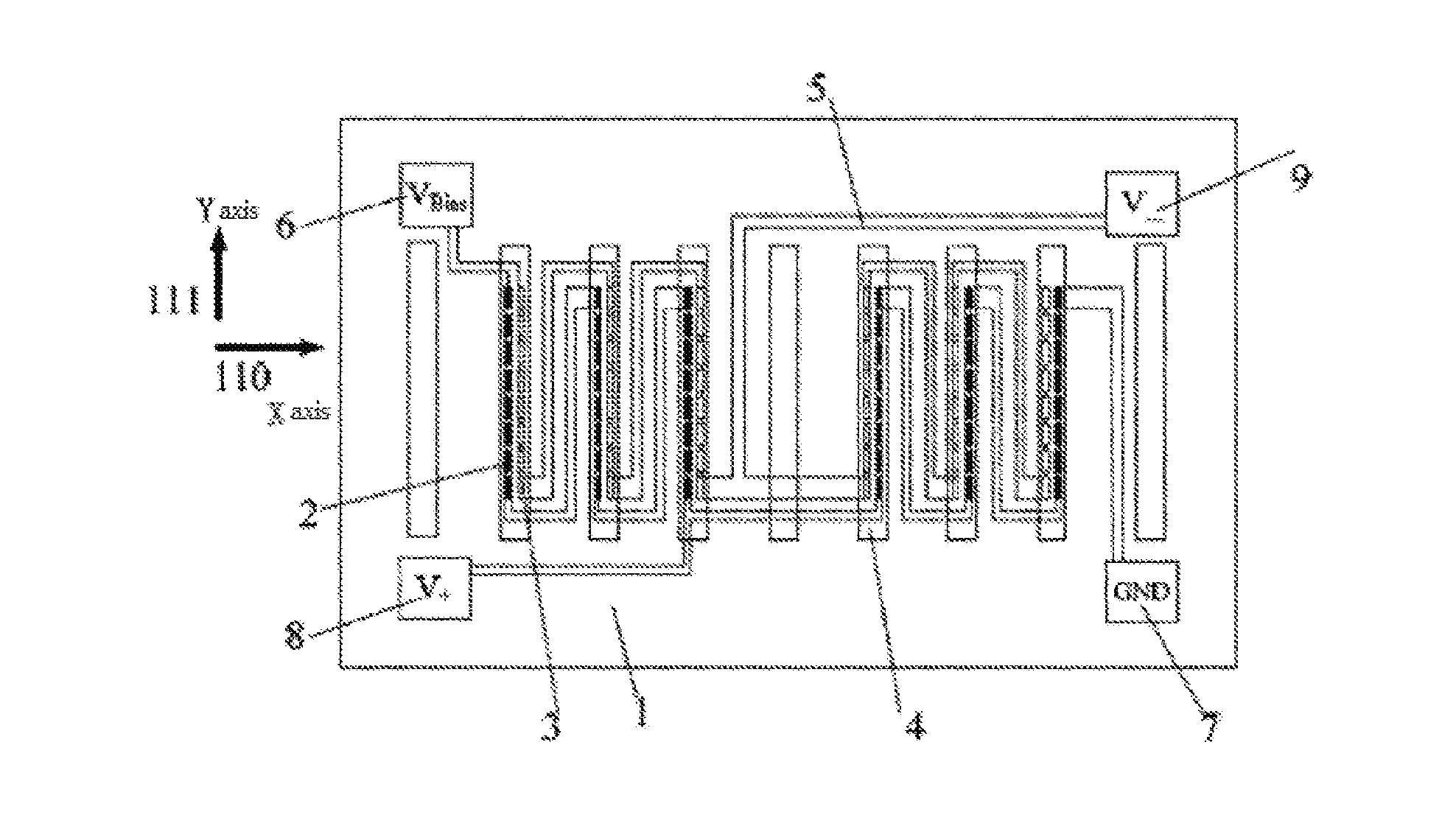
(2) A flux guide has previously been used in the art to convert a magnetic field from the Z-axis direction into magnetic field components in the X- and Y-axis directions. For example, Chinese Patent Application No. 201110098286.8 discloses a single-chip three-axis AMR sensor, which implements measurement of a magnetic field in the Z-axis direction by placing a flux guide above in-plane sensors. However, the flux guide does not completely cover all the in-plane sensors, such that the magnetic field in the Z-axis direction is not fully converted into theX- and Y-axis directions. In addition, the sensor design disclosed in that application does not permit the in-plane sensors to be densely packed in order to reduce noise, and it is also difficult to control temperature compensation and offsets thereof. In addition, Chinese Patent Application No. 201310202801.1 discloses a three-axis digital compass, which converts the Z-axis magnetic field component perpendicular to a plane by the distorting effects of a flux guide into a magnetic field component in the X-Y plane, and then separates the X-, Y-, and Z-axis magnetic field components of the external magnetic field by using a certain algorithm, and then converts the calculated components into a digital signal output. This design needs to use a specific algorithm for calculating the magnetic field in the Z-axis direction, which makes the sensor design more complicated, and since the design utilizes a referenced bridge structure, and the resulting sensor has an asymmetric output characteristic, offsets in the output of the sensor are generated.
(3) A substrate is micro-machined to form an inclined plane, onto which a sensor that partially senses the magnetic field in the Z-axis direction is deposited. Such a process is very complicated, has a low spatial efficiency, and may cause some shadowing effects in the deposition of the sensor, which may degrade the performance of the sensor.
(4) The magnetic field in the Z-axis direction is measured utilizing magnetic materials with perpendicular magnetic anisotropy. For example, US Patent Application US20130168787A1 discloses a magnetic sensor, which measures a Z-axis component of an external magnetic field by using a perpendicular magnetic anisotropy material, but the perpendicular magnetic anisotropy material has a high coercivity, and also low magnetoresistance.

Method used


Image

  • Single-chip z-axis linear magnetic resistance sensor
  • Single-chip z-axis linear magnetic resistance sensor
  • Single-chip z-axis linear magnetic resistance sensor

Examples


embodiments

[0049]FIG. 1 is a schematic structural view of a single-chip Z-axis linear magnetoresistive sensor of the present invention. It can be seen from FIG. 1 that, the sensor includes a substrate 1, a plurality of magnetoresistive sensing elements 2 and 3, a plurality of flux guides 4, electrically connected conductors 5, and solder pads 6-9. The solder pads 6-9 respectively serve as a power supply terminal VBias, a ground terminal GND, and voltage output terminals V+ and V−. The magnetoresistive sensing elements 2 and 3 are respectively located on two sides of the long axis beneath the flux guides 4, and the flux guides 4 can cover all the magnetoresistive sensing elements completely. Of course, the magnetoresistive sensing elements 2 and 3 can also be respectively located outside of the edges on two sides of the long axis beneath the flux guides 4. In this embodiment, although the magnetoresistive sensing elements are not placed beneath the three flux guides at the outmost of the left a...


PUM


Abstract

A single-chip Z-axis linear magnetoresistive sensor is provided. The sensor comprises a substrate, magnetoresistive sensing elements, and flux guides, wherein the magnetoresistive sensing elements are mutually electrically connected to form push arms and pull arms of a bridge; the push arms and the pull arms are alternately arranged, and the magnetoresistive sensing elements on the push arms and the pull arms are respectively located at two sides beneath the flux guides; the magnetization direction of a pinning layer of each magnetoresistive sensing element is the same and is in an X-axis direction. An external magnetic field in a Z-axis direction is converted into a magnetic field with components in an X-axis direction by the flux guides, and thus the magnetoresistive sensing elements beneath the flux guides can detect this component. The sensor has the advantages of the small size, simple manufacturing, simple packaging, high sensitivity, good linearity, wide operating range, low offset, good temperature compensation, and capability to measure high magnetic fields, etc.

Description

TECHNICAL FIELD[0001]The present invention relates to the field of sensor technology, and in particular, to a single-chip Z-axis linear magnetoresistive sensor.BACKGROUND ART[0002]As magnetoresistive sensor technology has, the applications of magnetoresitive sensors have become more extensive. Currently, magnetic sensors are widely used in cell phones and other mobile devices as electronic compass, and the market of such products is very sensitive to the cost and packaging size. For a two-dimensional magnetic field in an X-Y plane, measurement of the X and Y components of the magnetic field within the plane may be implemented by using two orthogonal sensors, but for the measurement on the magnetic field in a Z-axis direction there are many difficulties, as such, the following solutions are typically utilized:[0003](1) A separate single-axis planar magnetoresistive sensor is installed perpendicular to a two-axis planar sensor, but this manner has the following disadvantages:[0004]1. ...

Claims


Application Information

Patent Timeline
Patent Type & Authority Applications(United States)
IPC IPC(8): G01R33/09H01L43/08H01L27/22H01L43/02
CPCG01R33/09G01R33/091H01L43/08H01L43/02H01L27/22H10B61/00H10N59/00H10N50/10H10N50/80
Inventor DEAK, JAMES GEZA
Owner MULTIDIMENSION TECH CO LTD
Why Eureka
Try Eureka