Semiconductor device and method of manufacturing the same

a semiconductor and semiconductor technology, applied in the direction of semiconductor devices, semiconductor/solid-state device details, electrical devices, etc., can solve the problems of warpage, abnormal operation, warpage of semiconductor wafers, etc., and achieve the effect of reducing the warpage of wafers

Active Publication Date: 2016-08-11
AOI ELECTRONICS CO LTD
View PDF1 Cites 16 Cited by
  • Summary
  • Abstract
  • Description
  • Claims
  • Application Information

AI Technical Summary

Benefits of technology

[0016]An object of the present invention, which has been made to overcome the disadvantages described above, is to minimize the warpage of a wafer and semiconductor devices manufactured by division of the wafer into small pieces.
[0024]According to the first, second, third and fifth aspects of the present invention, a chip body is reinforced by a reinforcing layer, thus preventing the flexure of the chip body.

Problems solved by technology

This causes warpage of a semiconductor wafer and semiconductor chips produced by division of the semiconductor wafer into small pieces.
In particular, as the thickness of the semiconductor wafer decreases, its warpage increases.
For example, a robot hand cannot suck a wafer for transfer; a wafer cannot be sucked on a stage for processing or accommodated in a cassette slot; or a notch aligner centering the wafer to detect the orientation of the wafer cannot be focused on the wafer, leading to abnormal operation.
(A3) Prevention of the warpage of the structure of a chip (maintenance of uniformity or coplanarity): Individual chips from a warped wafer also warp and cause problems when implemented on devices or adversely affect their reliability.
A direct contact of a resin film with rewiring layers, UBM layers, or bump electrodes generates a high stress, which causes warpage.

Method used


Image

  • Semiconductor device and method of manufacturing the same
  • Semiconductor device and method of manufacturing the same
  • Semiconductor device and method of manufacturing the same

Examples


first embodiment

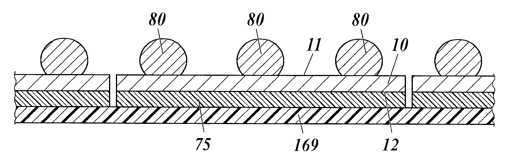
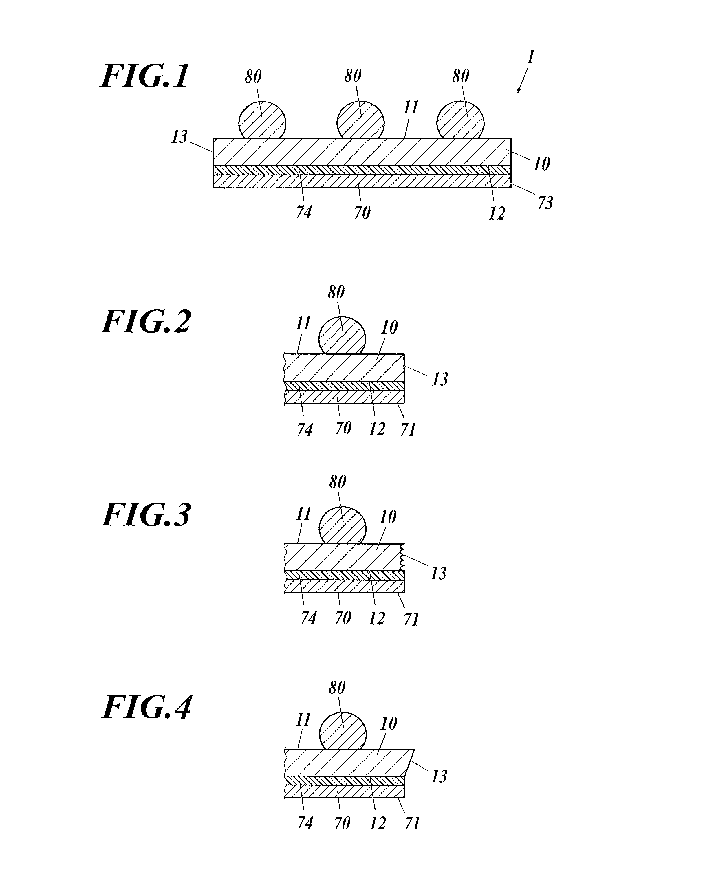
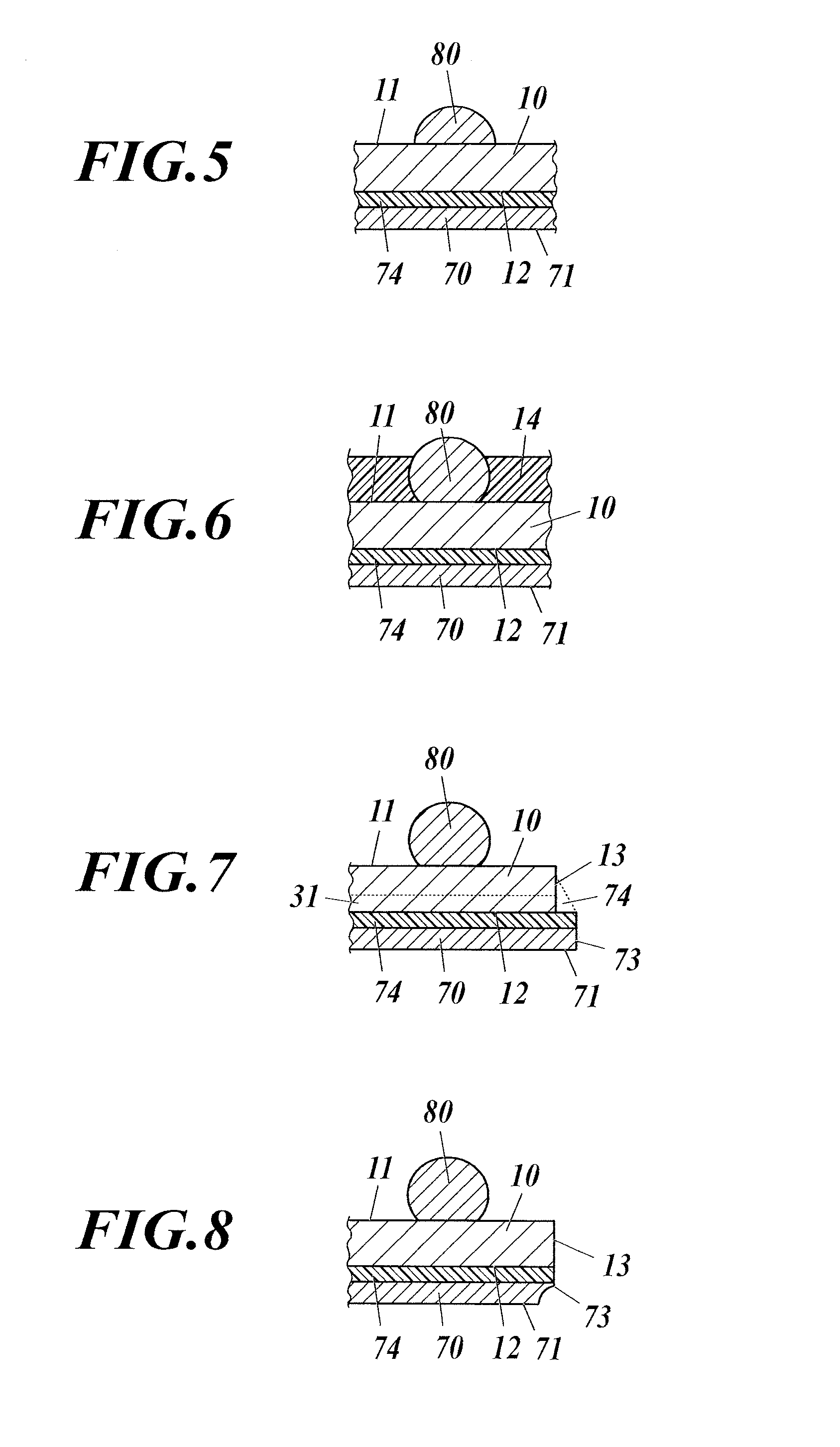
[0063]FIG. 1 is a schematic cross-sectional view of a semiconductor device 1.

[0064]The semiconductor device 1 is a separated semiconductor chip. The semiconductor device 1 includes a chip body 10, a reinforcing layer 70, a bonding layer 74, and solder bumps 80. The solder bumps 80 may be omitted or may be replaced with bumps composed of a material other than solder, such as electrodes for external connections.

[0065]The chip body 10 is manufactured by division of a wafer into pieces. The top and bottom faces of the chip body 10 have an area of, for example, 40 mm2 or more.

[0066]The chip body 10 includes a first main face 11 on its front side and a second main face 12 on its rear side. Although specific examples of the chip body 10 will be given later, the chip body 10 is one of a chip scale package (CSP) with rewiring layers and pillar terminals (see FIG. 9), a CSP with rewiring layers and UBM layers (see FIG. 10), and a CSP with terminals (see FIG. 11). A process for manufacturing a...

second embodiment

[0128]A method of manufacturing the semiconductor device 1 will now be described.

[0129](1) Wafer Preparing Process (Wafer Fabricating Process)

[0130]A wafer 110 provided with multiple solder bumps 80 is prepared, as shown in FIG. 12A. The wafer 110 is not yet divided into chip bodies 10. The wafer 110 can be manufactured by different methods depending on the type of the chip body 10: a CSP with rewiring layers and pillar terminals, a CSP with rewiring layers and UBM layers, or a CSP with terminals. The method of manufacturing the wafer 110 will now be described for each type.

[0131](1-1) In the Case of the Chip Body 10 being a CSP with Rewiring Layers and Pillar Terminals

[0132]With reference to FIG. 14A, a device wafer 131 is prepared. The device wafer 131 is a substrate larger than a device substrate 31 and is divided into multiple device substrates 31 along designed dividing lines 131L (also called “dicing lines”). The device wafer 131 is thicker than the device substrate 31 and thi...

third embodiment

[0204]A method of manufacturing the semiconductor device 1 will now be described.

[0205]“(1) Wafer preparing process”, “(2) Support plate bonding process”, “(3) Wafer thinning process”, and “(5) Reinforcing layer preparing process” are performed as in the second embodiment (see FIGS. 12A to 12C, 13E to 13F, and 14A to 17K).

[0206](1a) Reinforcing Layer Bonding Process

[0207]With reference to FIG. 21A, the reinforcing layer 70 is bonded to the second main face 112 of the wafer 110 via the bonding layer 74 such that the reinforcing layer 70 is positioned not across any designed dividing line 131L but within a grid cell defined by the designed dividing lines 131L.

[0208]The detailed description of the bonding of the reinforcing layer 70 is omitted as it is the same as that of “(6) Reinforcing layer bonding process” in the second embodiment.

[0209](2a) Wafer Dividing Process

[0210]The wafer 110 is cut by chemical means. More specifically, the wafer 110 is divided into multiple chip bodies 10 ...


PUM


Abstract

A method of manufacturing a semiconductor device, including steps of: (a) bonding a support plate to a first main face of a wafer, the first main face having an integrated circuit disposed thereon; (b) thinning the wafer by polishing or grinding a second main face after step (a), the second main face being opposite to the first main face; (c) dividing the wafer into multiple chip bodies concurrently with or after step (b); (d) bonding multiple reinforcing layers to second main faces of the respective chip bodies after step (c); and (e) removing the support plate after step (d).

Description

BACKGROUND OF THE INVENTION[0001]1. Field of the Invention[0002]The present invention relates to a semiconductor device and a method of manufacturing the semiconductor device.[0003]2. Description of Related Art[0004]A typical method of packaging semiconductor chips is wafer-level packaging (WLP). The WLP method involves applying a liquid resin to a semiconductor wafer, curing the liquid resin into a sealing layer, and dividing the semiconductor wafer together with the sealing layer into small pieces (See Japanese Unexamined Patent Application Publication No. 2011-176069, Japanese Patent No. 4725638, and Japanese Patent No. 4725639). This method enables the production of small packages with substantially the same size as that of semiconductor chips.[0005]A thermosetting liquid resin shrinks when it is cured. This causes warpage of a semiconductor wafer and semiconductor chips produced by division of the semiconductor wafer into small pieces. In particular, as the thickness of the sem...

Claims


Application Information

Patent Timeline
Patent Type & Authority Applications(United States)
IPC IPC(8): H01L21/56H01L21/304H01L21/306H01L23/528H01L21/308H01L21/768H01L23/31H01L21/683H01L21/78
CPCH01L21/304H01L21/30625H01L21/78H01L21/3081H01L21/6835H01L23/3107H01L23/528H01L2221/68327H01L21/56H01L21/768H01L21/6836H01L23/3114H01L23/525H01L23/562H01L24/11H01L29/0657H01L2221/6834H01L2221/68381H01L2224/03912H01L2224/0401H01L2224/05569H01L2224/05571H01L2224/05572H01L2224/11462H01L2224/1147H01L2224/1181H01L2224/1184H01L2224/11849H01L2224/1191H01L2224/13082H01L2224/131H01L2224/13147H01L2224/94H01L2224/03H01L2224/11H01L2924/00014H01L2924/014H01L2924/00012H01L24/12
Inventor SHIOTA, JUNJIKONO, ICHIRO
Owner AOI ELECTRONICS CO LTD
Why Eureka
Try Eureka