Organic light emitting diode display device and method for manufacturing the same

a light-emitting diode and display device technology, applied in the field of display, can solve the problems of low light-emitting efficiency of amoled, low external quantum efficiency of light-emitting devices, and large loss of light-emitting devices, so as to improve the light-emitting efficiency of oled display devices, improve the external quantum efficiency of light-emitting devices, and reduce the scattering effect of films for ligh

Active Publication Date: 2016-09-01
BOE TECH GRP CO LTD +1
View PDF5 Cites 3 Cited by
  • Summary
  • Abstract
  • Description
  • Claims
  • Application Information

AI Technical Summary

Benefits of technology

[0024]In the OLED display device and the method for manufacturing the same, a vertical projection of the luminescent layer of the luminescent layer on the array substrate defines the pixel opening area, both a vertical projection of the hole transport layer on the array substrate and a vertical projection of the electron transport layer on the array substrate partially cover the pixel opening area; the vertical projection of the hole transport layer on the ar

Problems solved by technology

During the whole luminescent process, when the light is transmitted in the above mentioned layers, it is partially absorbed and scattered due to the optical waveguide effect; the light should be transmitted out of the light emitting device t

Method used


Image

  • Organic light emitting diode display device and method for manufacturing the same
  • Organic light emitting diode display device and method for manufacturing the same
  • Organic light emitting diode display device and method for manufacturing the same

Examples


embodiment 1

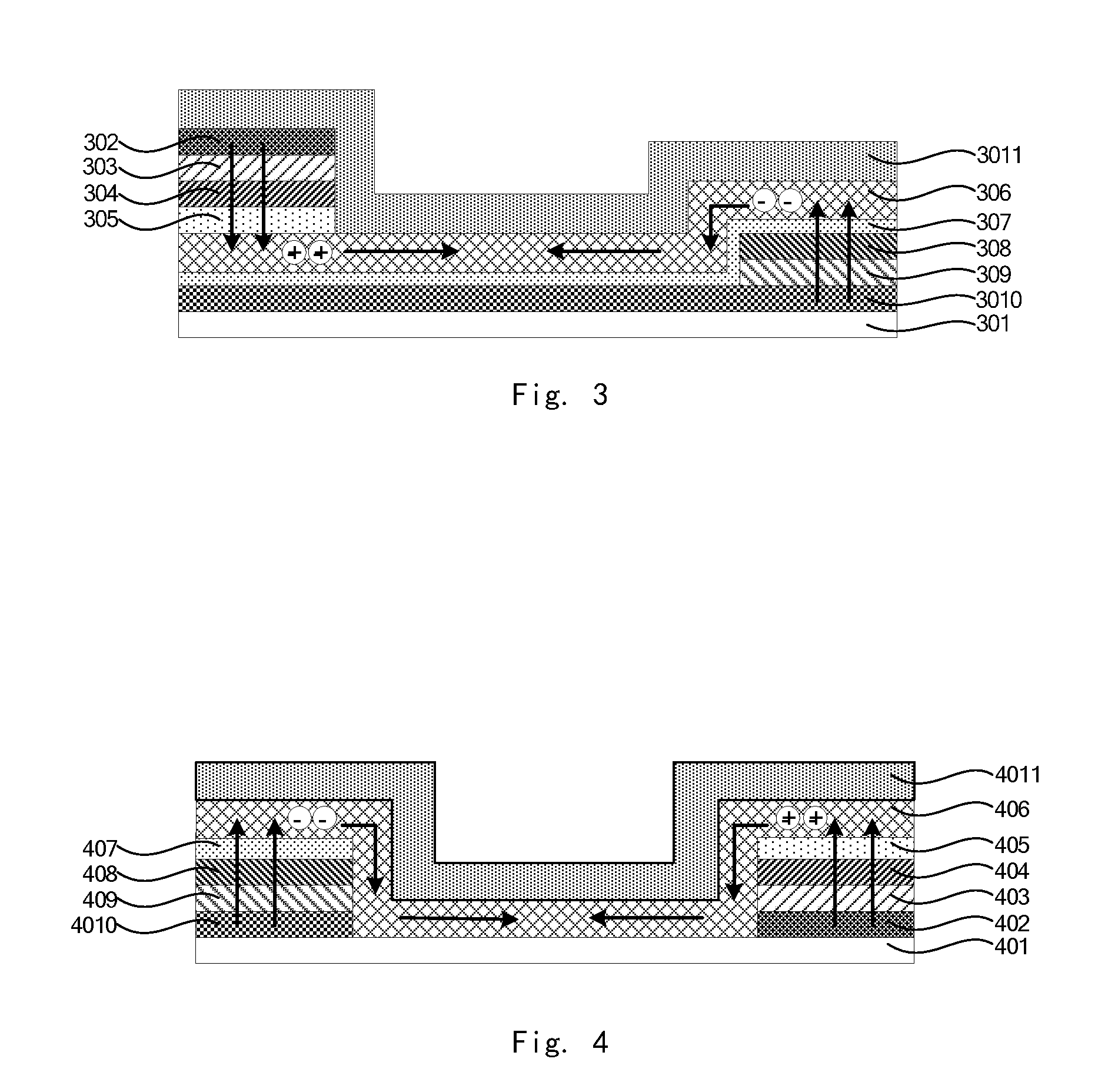
[0032]An embodiment of the present invention provides an OLED display device; the organic light emitting diode display device comprises:

[0033]an array substrate comprising a plurality of pixel opening areas;

[0034]a light emitting device located in each of the pixel opening areas on the array substrate; wherein

[0035]the light emitting device comprises: a hole transport layer, a luminescent layer and an electron transport layer; wherein

[0036]a vertical projection of the luminescent layer on the array substrate defines the pixel opening area;

[0037]the hole transport layer and the electron transport layer are located on different sides of the luminescent layer respectively, or the hole transport layer and the electron transport layer are located on the same side of the luminescent layer;

[0038]both a vertical projection of the hole transport layer on the array substrate and a vertical projection of the electron transport layer on the array substrate partially cover the pixel opening area...

embodiment 2

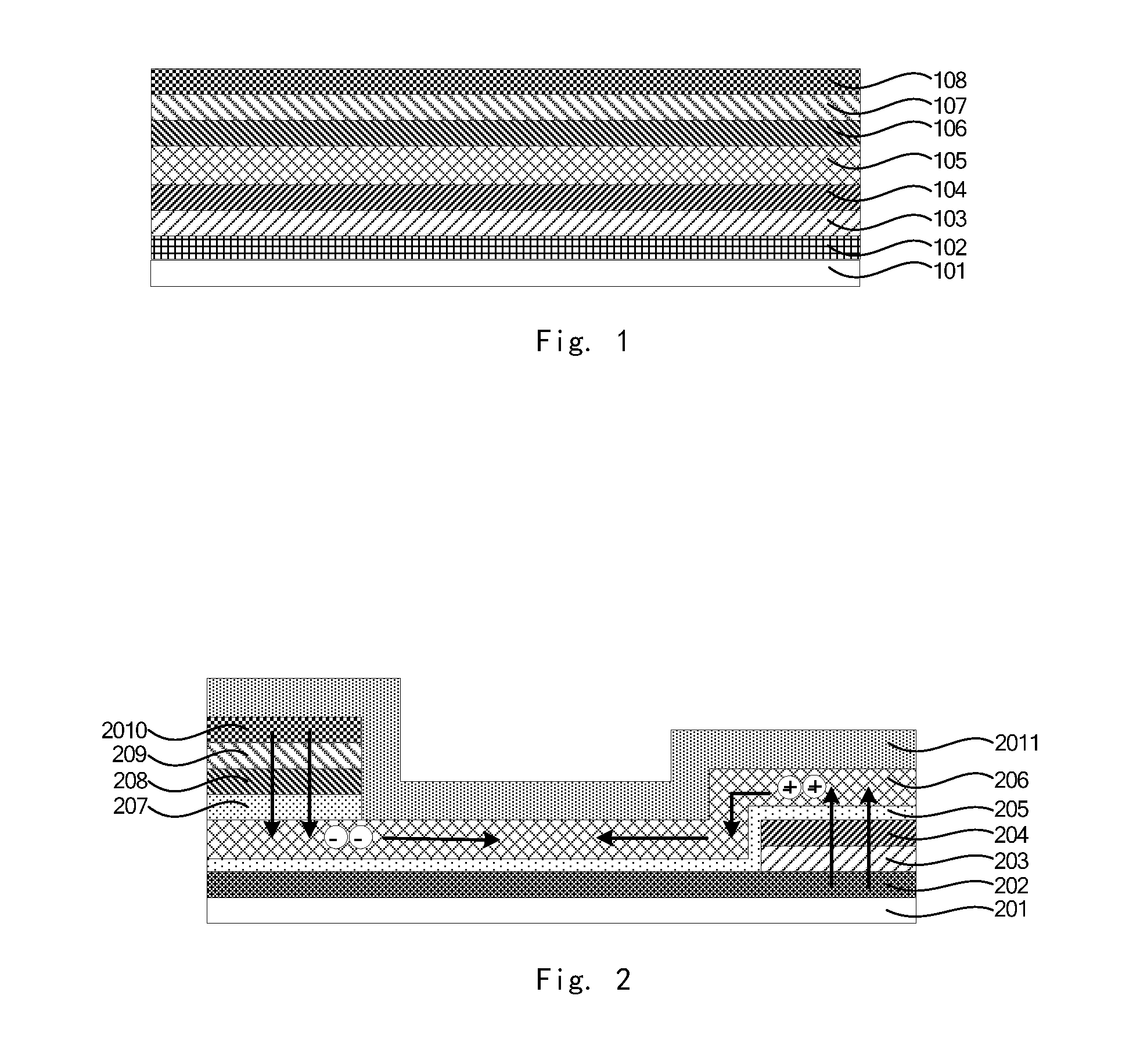
[0048]Based on the OLED display device provided by the Embodiment 1, the OLED display device provided by the embodiment can also comprise: a hole injection layer located on a side of the hole transport layer departing from the luminescent layer, and an electron injection layer located on a side of the electron transport layer departing from the luminescent layer; the hole injection layer completely overlaps with the hole transport layer; the electron injection layer completely overlaps with the electron transport layer; an anode located on a side of the hole injection layer departing from the luminescent layer, and a cathode located on a side of the electron injection layer departing from the luminescent layer.

[0049]That is to say, the light emitting device can be divided into a luminescent layer for the recombination of hole and electron, a hole unit for transporting holes to the luminescent layer, and an electron unit for transporting electrons to the luminescent layer. The hole t...

embodiment 3

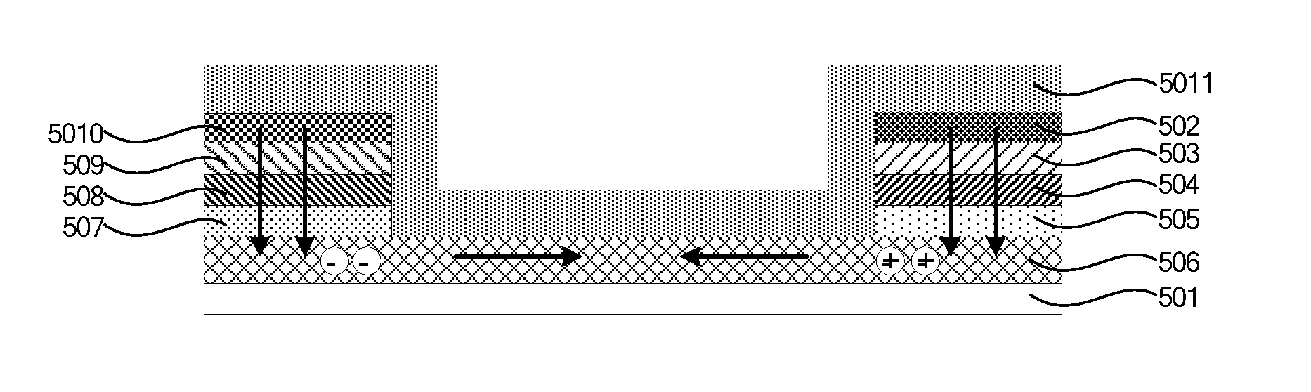
[0094]When the hole transport layer and electron transport layer are preferably located on the same side of the luminescent layer (i.e., the hole unit comprising the hole transport layer, the hole injection layer and the anode is located on the same side of the luminescent layer as the electron unit comprising the electron transport layer, the electron injection layer and the cathode), the anode can be completely overlapped with the hole transport layer, the cathode can be completely overlapped with the electron transport layer (i.e., the vertical projections of the anode and the cathode on the luminescent layer partially cover the pixel opening area, and completely overlap with the vertical projections of the hole transport layer and the electron transport layer on the luminescent layer respectively).

[0095]As shown in FIG. 4, taking an OLED display device as an example, in which both the hole unit and electron unit are located on the lower side of the luminescent layer 406. In part...


PUM


Abstract

The embodiments of the present invention provide an organic light emitting diode display device and a method for manufacturing the same. The organic light emitting diode display device comprises: an array substrate comprising a plurality of pixel opening areas; a light emitting device located in each of the pixel opening areas on the array substrate; wherein the light emitting device comprises: a hole transport layer, a luminescent layer and an electron transport layer; wherein a vertical projection of the luminescent layer on the array substrate defines the pixel opening area; the hole transport layer and the electron transport layer are located on different sides of the luminescent layer respectively, or the hole transport layer and the electron transport layer are located on the same side of the luminescent layer; both a vertical projection of the hole transport layer on the array substrate and a vertical projection of the electron transport layer on the array substrate partially cover the pixel opening area; the vertical projection of the hole transport layer on the array substrate and the vertical projection of the electron transport layer on the array substrate do not overlap with each other. The display device and the method for manufacturing the same can reduce the number of the layers required for transmitting the light out of the light emitting device, reducing the loss of the light due to the absorption and scattering of the films; improving the external quantum efficiency of the light emitting device; thereby improving the light emitting efficiency of the display device.

Description

FIELD OF THE INVENTION[0001]The present invention relates to the technical field of display, in particular to an organic light emitting diode (OLED) display device and a method for manufacturing the same.BACKGROUND OF THE INVENTION[0002]With the continuous development of display technology, OLED display device has become the main trend of the next generation display device due to the advantages of light weight, high contrast, high color gamut, low power consumption, and realizability of flexible display.[0003]Among the OLED display devices, active matrix organic light emitting diode (AMOLED) display has a quick response, and can meet the requirements of display devices with various sizes, so it has attracted attention of many enterprises. AMOLED display device typically comprises an array substrate and light emitting devices, wherein the light emitting devices are mainly realized by a fine metal mask, of which the implementation has become increasingly mature, enabling the mass prod...

Claims


Application Information

Patent Timeline
IPC IPC(8): H01L27/32H01L51/52H01L51/56H01L51/50
CPCH01L27/326H01L51/5072H01L51/5253H01L2227/323H01L51/5056H01L51/5096H01L51/56H10K50/18H10K50/80H10K50/11H10K71/00H10K59/121H10K50/15H10K50/16H10K50/156H10K50/166H10K50/844H10K59/1213H10K59/1201
Inventor ZHENG, JINZHONG
Owner BOE TECH GRP CO LTD
Why Eureka
Try Eureka