Supercharge Your Innovation With Domain-Expert AI Agents!

Method of Separating a Carrier-Workpiece Bonded Stack

a carrierworkpiece and stack technology, applied in the field of carrierworkpiece bonding stack separation, can solve the problems of increasing capacitance, requiring thicker transmission lines, and large ic footprin

Active Publication Date: 2016-11-17
MICRO MATERIALS INC
View PDF6 Cites 6 Cited by
  • Summary
  • Abstract
  • Description
  • Claims
  • Application Information

AI Technical Summary

Benefits of technology

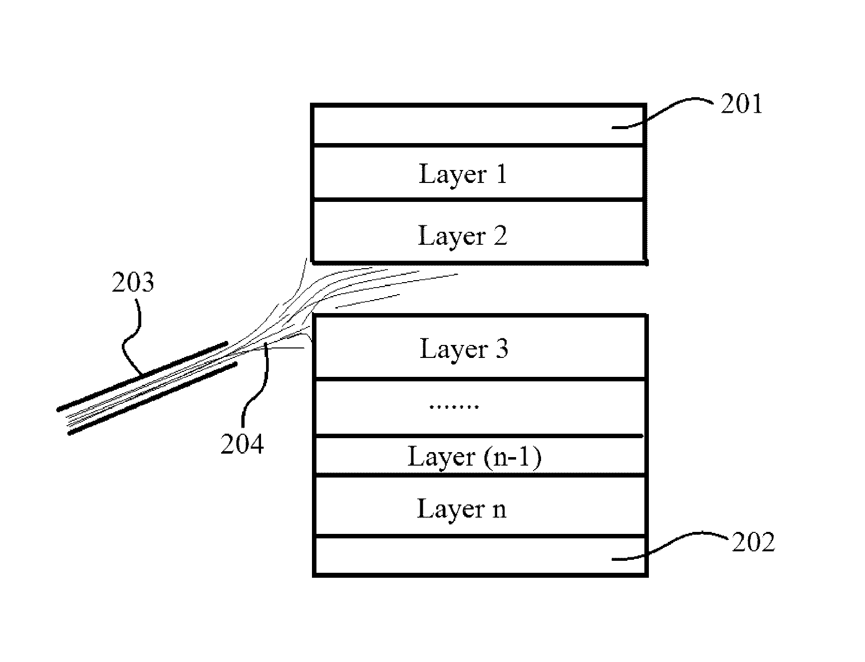
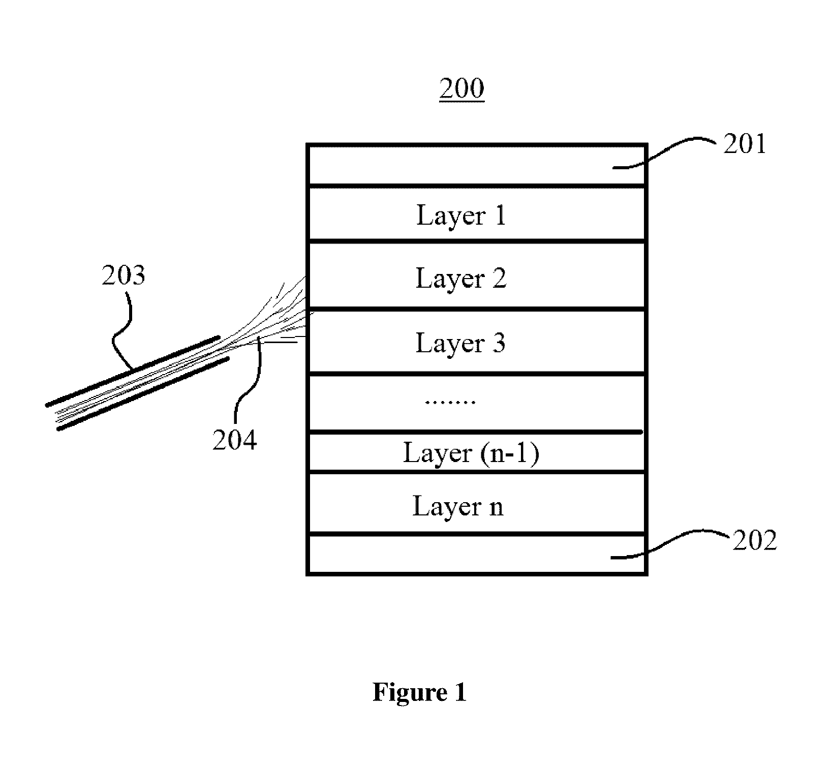
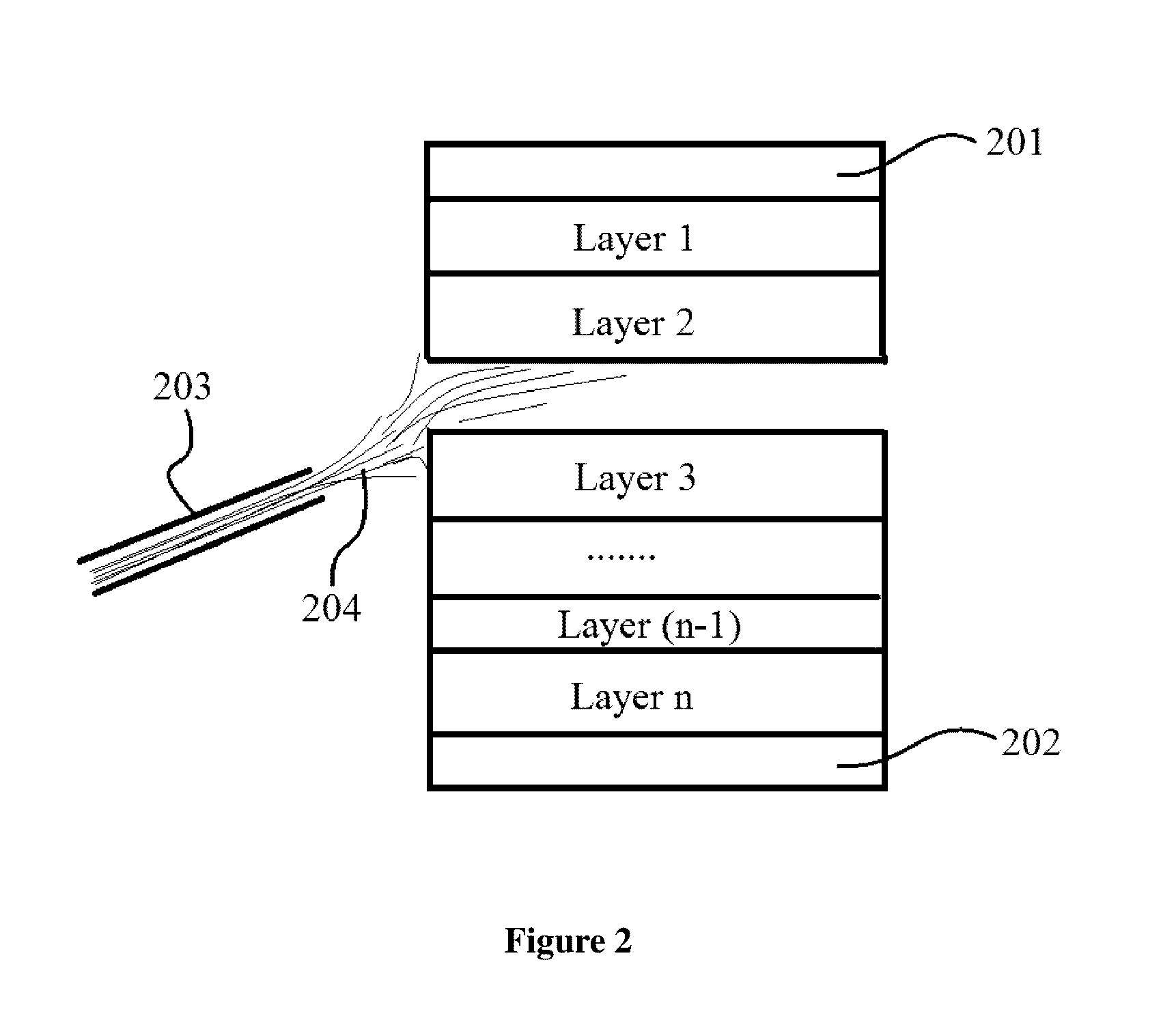
The invention provides a method for joining two layers together with a gas jet. An additional step can be added before step (iii) which mechanically or chemically disrupts or destroys a portion of the outer periphery at the junction of two adjacent layers. This makes the later steps easier, as the user can use a gas stream with lower pressure and / or flow rate. The technical effect is improved precision and efficiency in joining layers with a gas jet.

Problems solved by technology

Thick wafers cause an increase in capacitance, requiring thicker transmission lines, and, in turn, a larger IC footprint.
Without thinning, it would be nearly impossible to form backside electrical contacts that connect with front-side circuitry by passing the connections through the wafer.
Device wafers that have been thinned to less than 100 microns, and especially those thinned to less than 60 microns, are extremely fragile and must be supported over their full dimensions to prevent cracking and breakage.
Various wafer wands and chucks have been developed for transferring ultra-thin device wafers, but the problem still exists on how to support the wafers during back-grinding and TSV-formation processes, because these steps impose high thermal and mechanical stresses on the device wafer as it is being thinned or after thinning.
In debonding the bonded stack, particularly in an automatic process, complicated mechanical mechanisms such as robot arms must be employed to manipulate the stack using strong but non-uniform mechanical force, to execute motions like sliding, lifting, and twisting.
As thinned wafers are extremely fragile, defects associated with this approach include device wafer breakage and damage within the microscopic circuitry of individual devices, which lead to device failure and yield loss.
Moreover, complicated mechanical mechanisms also suffer from the disadvantages of higher cost, difficult operation, and lower efficiency.

Method used


Image

  • Method of Separating a Carrier-Workpiece Bonded Stack
  • Method of Separating a Carrier-Workpiece Bonded Stack
  • Method of Separating a Carrier-Workpiece Bonded Stack

Examples


example 1

Device Wafer Coating

[0078]A silicon device wafer (i.e. workpiece 60 or wafer 50) was placed onto a vacuum chuck in a WS-400 spin coater (available from Laurell Technologies). Approximately 2 ml of Z-BOND 601 Silicone composition (available from Micro Materials Inc. (MMI), 10080 Willow Creek Road, San Diego, Calif. 92131) was needle dispensed onto the center of the wafer. The wafer was then rotated at 500 rpm for 10 seconds, 1000 rpm for 5 seconds, 2000 rpm for 10 seconds, and 600 rpm for 5 seconds, and the rotation was then stopped. The Z-BOND 601 formed a uniform wet layer on the device wafer after the spin coating. The thickness of the wet Z-BOND 601 layer (i.e. adhesive layer 40) is about 15 μm.

example 2

Carrier Wafer Coating and Formation of Support 10

[0079]A silicon dummy wafer was used as the carrier wafer, and it was placed onto a vacuum chuck in a WS-400 spin coater. Approximately 2 ml of Z-COAT 150 polyethersulfone composition (available from Micro Materials Inc., 10080 Willow Creek Road, San Diego, Calif. 92131) was needle dispensed onto center of the carrier wafer. Then wafer was rotated at 700 rpm for 5 seconds, 1500 rpm for 10 seconds, and 500 rpm for 5 seconds, before the rotation was stopped. The Z-COAT 150 formed a uniform wet layer on the carrier wafer after the spin coating. The thickness of the wet Z-COAT 150 layer right after the spin coating is approximately 12 μm.

[0080]The carrier with wet Z-COAT 150 layer was then placed on a hot plate of 80° C. for 10 minutes. The Z-COAT 150 started to form a dry layer on the carrier wafer during the heating. Carrier was then moved to a second hot plate of 200° C. for 7 minutes, then to third hot plate of 350° C. for 10 minutes,...

example 3

Wafer Bonding and Thermal Stability

[0081]The wafer bonder used in this example is Z-BT200 bonder commercially available from Micro Materials Inc., 10080 Willow Creek Road, San Diego, Calif. 92131. Support 10 from Example 2 in which the supporting surface 21 and the isolation film 30 are bonded together, and wafer 50 from Example 1 in which its engaging surface 51 is bonded to the adhesive layer 40, are then pressed together, so that the second side 32 of the isolation film 30 is in contact with the first side 41 of the adhesive layer 40. The bonding was conducted at a temperature of 120° C. with 1 kg force applied for 4 minutes in vacuum of 0.1 millibars to form a bonded wafer stack 100. The wafer stack was visually inspected and no voids were observed. Thermal stability was evaluated by placing a bonded wafer stack on to a hot plate set to 350° C., after which the wafer stack were visually inspected, and no blister, crack, rupture, color change or other visual defects on the carrie...


PUM


Abstract

The present invention provides a method of separating a bonded stack utilizing the force generated by a gas jet. The stack includes a carrier and a thinned workpiece such as device wafer that are bonded together through one or more layers therebetween. The gas jet can separate two adjacent layers having peeling strength therebetween in the range of from 0.01 to 50.0 g / cm. The invention can simplify the procedure and provide high throughput in separating thinned wafer from its carrier.

Description

CROSS-REFERENCE TO RELATED U.S. APPLICATIONS[0001]This application claims the benefit of priority under the Paris Convention based on Chinese Application No. 201510247398.3 filed on May 14, 2015. The entire content of the patent application is incorporated by reference in its entirety.STATEMENT REGARDING FEDERALLY SPONSORED RESEARCH OR DEVELOPMENT[0002]Not applicable.NAMES OF PARTIES TO A JOINT RESEARCH AGREEMENT[0003]Not applicable.REFERENCE TO AN APPENDIX SUBMITTED ON COMPACT DISC[0004]Not applicable.FIELD OF THE INVENTION[0005]The present invention generally relates to a method of separating a carrier-workpiece bonded stack using one or more gas jets. The invention is particularly useful for processing a workpiece made of any brittle material, such as semiconductor wafers e.g. silicon and gallium arsenide, a rock crystal wafer, sapphire and glass; and for making thin products such as optical lens, thin silicon wafer, thin LCD glass, thin rock crystal wafer, thin metal plate, thin...

Claims


Application Information

Patent Timeline
IPC IPC(8): B32B43/00B32B37/06B32B38/10
CPCB32B43/006B32B37/06B32B38/10H01L21/6835H01L2221/68381B32B2457/14H01L21/67092Y10T156/1111Y10T156/1116Y10T156/1137Y10T156/1153Y10T156/1158Y10T156/1184Y10T156/1911Y10T156/1917Y10T156/1939Y10T156/1967
Inventor TANG, HAOZENG, YUSHEN
Owner MICRO MATERIALS INC
Features
  • R&D
  • Intellectual Property
  • Life Sciences
  • Materials
  • Tech Scout
  • Unparalleled Data Quality
  • Higher Quality Content
  • 60% Fewer Hallucinations
Learn More