Method of separating a carrier-workpiece bonded stack
a carrierworkpiece and stack technology, applied in the field of carrierworkpiece bonding stack separation, can solve the problems of increasing capacitance, requiring thicker transmission lines, and large ic footprin
- Summary
- Abstract
- Description
- Claims
- Application Information
AI Technical Summary
Benefits of technology
Problems solved by technology
Method used
Image

Examples
example 1
fer Coating
[0078]A silicon device wafer (i.e. workpiece 60 or wafer 50) was placed onto a vacuum chuck in a WS-400 spin coater (available from Laurell Technologies). Approximately 2 ml of Z-BOND 601 Silicone composition (available from Micro Materials Inc. (MMI), 10080 Willow Creek Road, San Diego, Calif. 92131) was needle dispensed onto the center of the wafer. The wafer was then rotated at 500 rpm for 10 seconds, 1000 rpm for 5 seconds, 2000 rpm for 10 seconds, and 600 rpm for 5 seconds, and the rotation was then stopped. The Z-BOND 601 formed a uniform wet layer on the device wafer after the spin coating. The thickness of the wet Z-BOND 601 layer (i.e. adhesive layer 40) is about 15 μm.
Example 2: Carrier Wafer Coating and Formation of Support 10
[0079]A silicon dummy wafer was used as the carrier wafer, and it was placed onto a vacuum chuck in a WS-400 spin coater. Approximately 2 ml of Z-COAT 150 polyethersulfone composition (available from Micro Materials Inc., 10080 Willow Cree...
example 3
ding and Thermal Stability
[0081]The wafer bonder used in this example is Z-BT200 bonder commercially available from Micro Materials Inc., 10080 Willow Creek Road, San Diego, Calif. 92131. Support 10 from Example 2 in which the supporting surface 21 and the isolation film 30 are bonded together, and wafer 50 from Example 1 in which its engaging surface 51 is bonded to the adhesive layer 40, are then pressed together, so that the second side 32 of the isolation film 30 is in contact with the first side 41 of the adhesive layer 40. The bonding was conducted at a temperature of 120° C. with 1 kg force applied for 4 minutes in vacuum of 0.1 millibars to form a bonded wafer stack 100. The wafer stack was visually inspected and no voids were observed. Thermal stability was evaluated by placing a bonded wafer stack on to a hot plate set to 350° C., after which the wafer stack were visually inspected, and no blister, crack, rupture, color change or other visual defects on the carrier or wafe...
example 4
onding—Gas Jetting
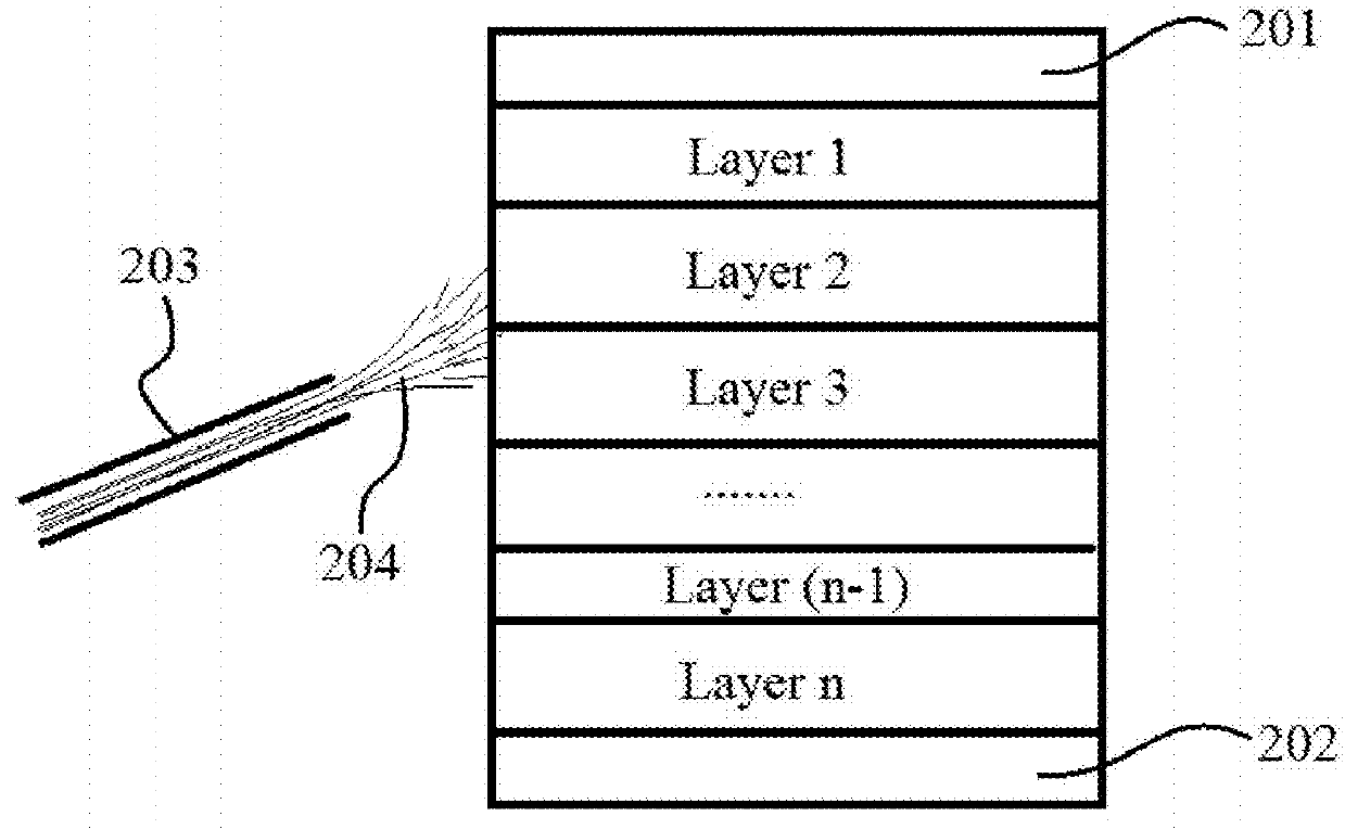
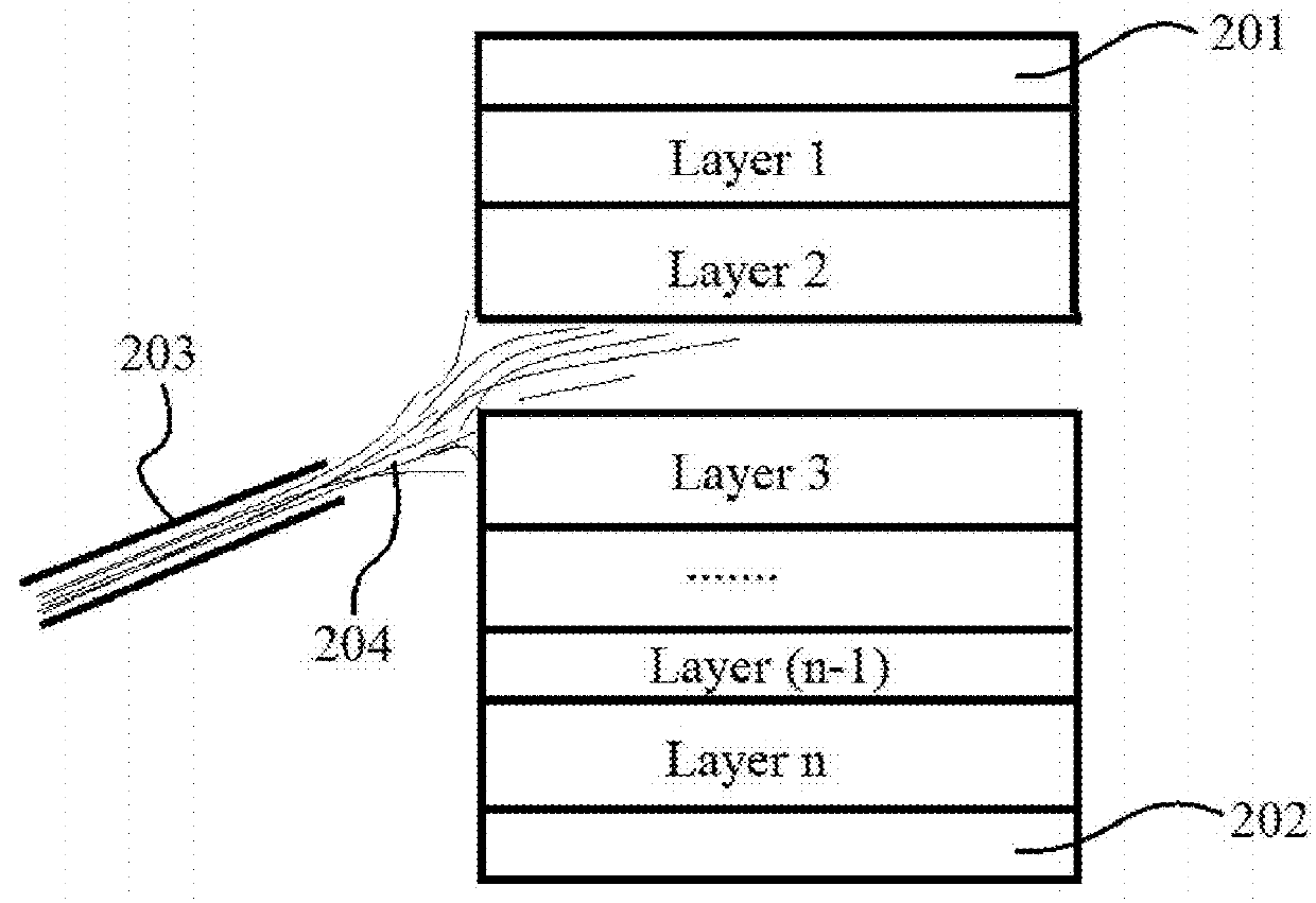
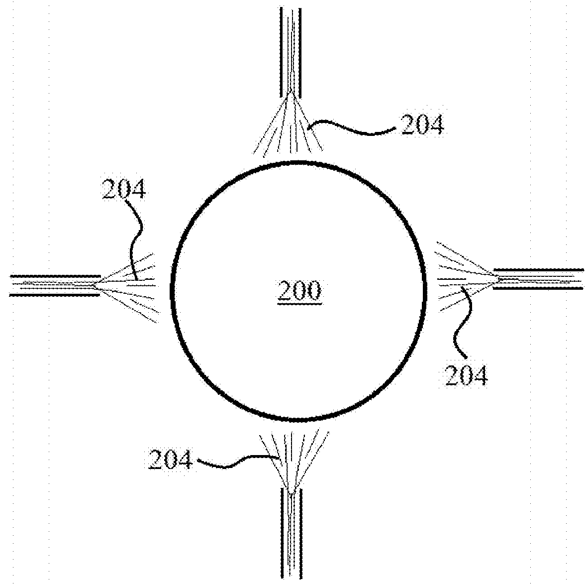
[0082]Wafer stack 100 was separated using automatic Wafer Debonder Z-D200A commercially available from Micro Materials Inc., 10080 Willow Creek Road, San Diego, Calif. 92131. First, the thinned device wafer was laminated on a wafer dicing film (Adwill D175, available from Lintec) on a metal frame. The laminated wafer stack was placed in Z-D200A with carrier wafer facing up. A sharp blade was automatically aligned to the interface between isolation film and carrier wafer by machine recognition. The blade is designed to have a controlled compressed gas channel. The blade was controlled to move toward the interface until it touched the interface, and then the blade was inserted 0.3 mm further in between the isolation film and the carrier wafer. A stream of high flow compressed gas (air) was shoot (or blew) from the channel in the blade toward the gap between the isolation film and supporting carrier wafer for about 10 seconds. The device wafer was then completely sepa...
PUM
| Property | Measurement | Unit |
|---|---|---|
| central angle | aaaaa | aaaaa |
| thickness | aaaaa | aaaaa |
| dihedral angle | aaaaa | aaaaa |
Abstract
Description
Claims
Application Information