Modular interconnects for gate-all-around transistors

a transistor and module technology, applied in semiconductor devices, semiconductor/solid-state device details, diodes, etc., can solve the problems of awkward electrical contact with the lowest terminal of the vertical gaa fet, i.e., the source or the drain, and achieve the effect of facilitating building complexes

Active Publication Date: 2017-01-05
STMICROELECTRONICS SRL
View PDF4 Cites 46 Cited by
  • Summary
  • Abstract
  • Description
  • Claims
  • Application Information

AI Technical Summary

Benefits of technology

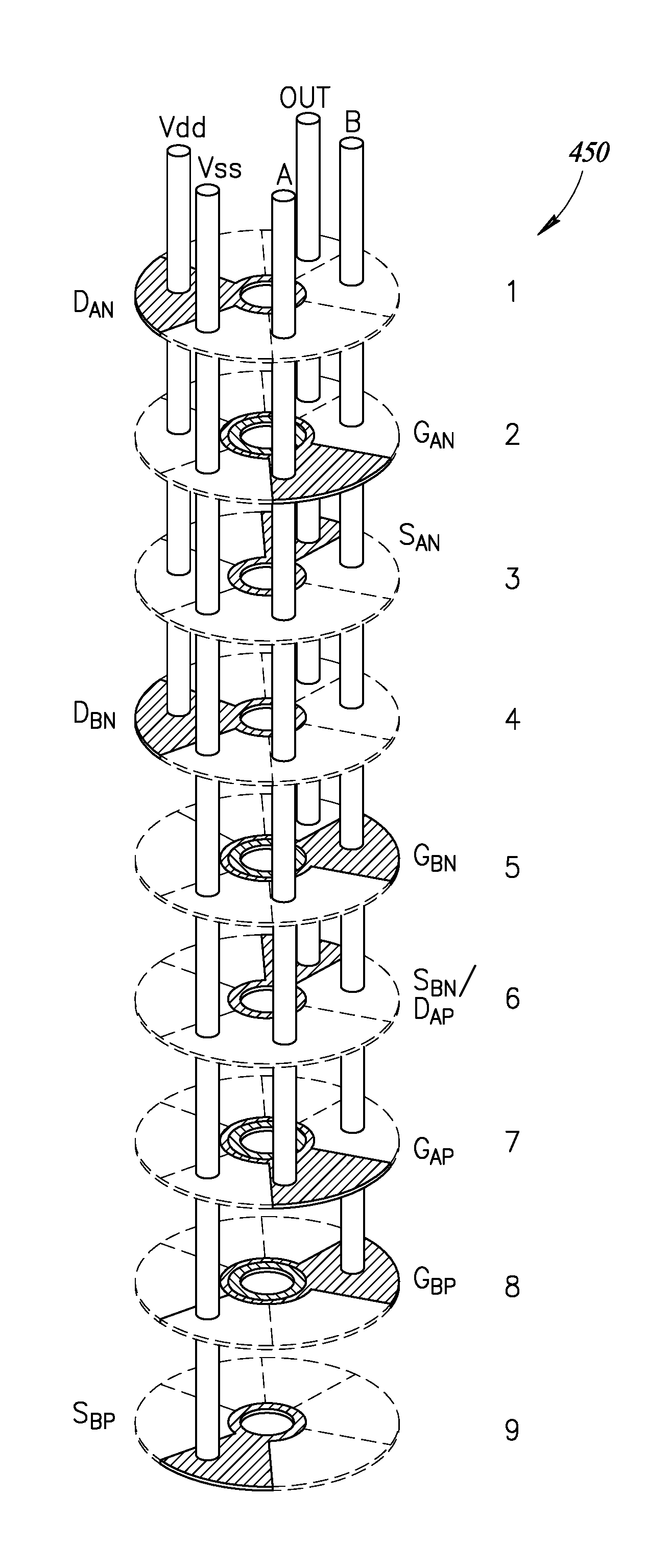
[0009]The modular interconnect structure facilitates building complex, yet compact, integrated circuits from vertical GAA FETs. Vertical NAND gate and NOR gate designs are disclosed that can be used as building blocks for creating all types of logic gates, and thus to carry out any desired Boolean logic function using a vertical GAA FET architecture. In some configurations, it is advantageous to stack vertical GAA FETs on top of one another. Stacked vertical GAA FETs are made possible by the modular interconnect structure. In addition, vertical GAA FET versions of specialized transistors are presented, including a vertical GAA tunneling field effect transistor (VGAA TFET), a vertical GAA silicon-oxide-nitride-oxide-silicon (VGAA SONOS) device, a vertical GAA silicon-on-insulator (VGAA SOD device, and a vertical GAA static induction transistor (VGAA SIT). The modular interconnect structure disclosed herein permits any of these VGAA devices to be integrated on a silicon substrate using standard CMOS processes.

Problems solved by technology

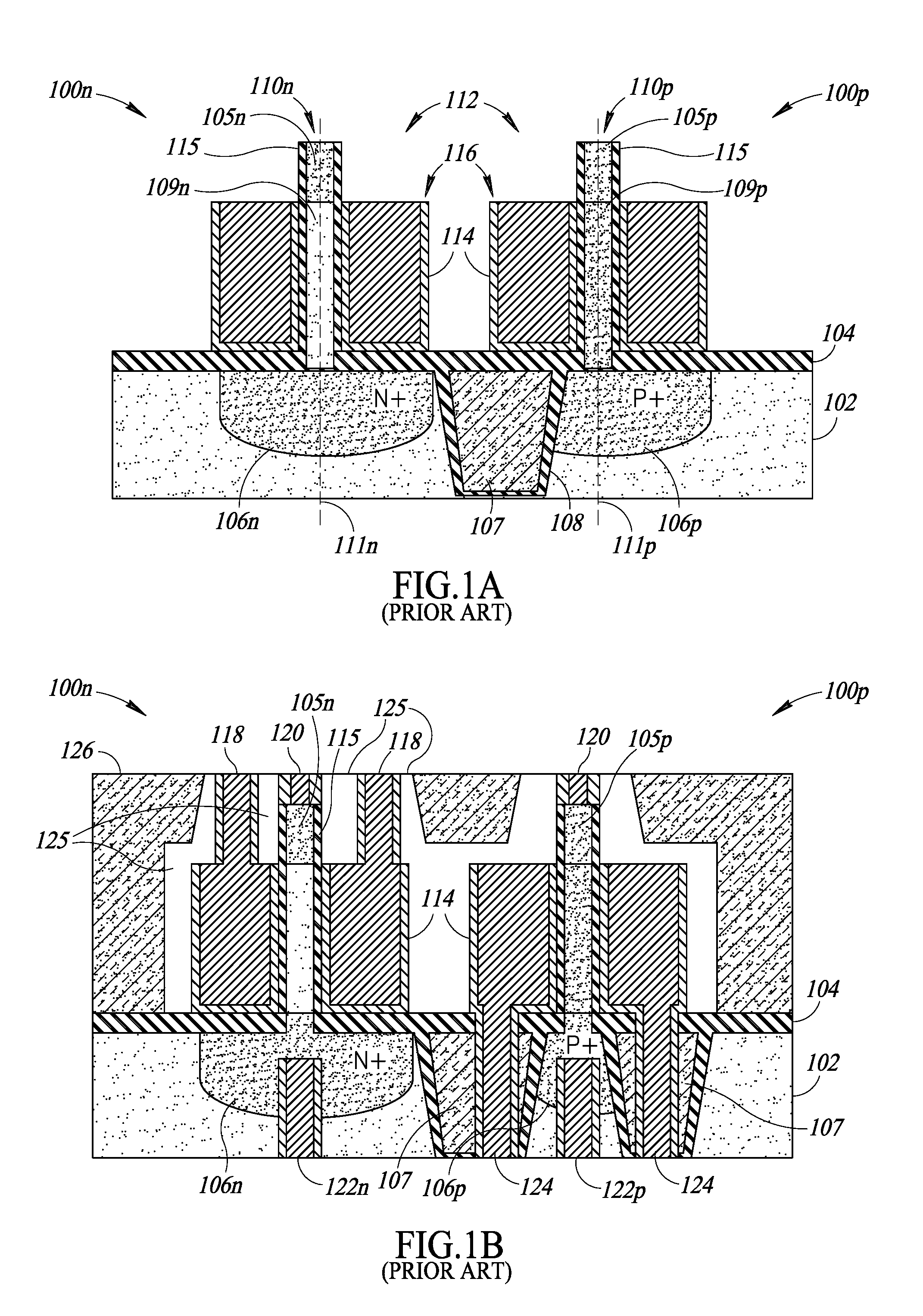
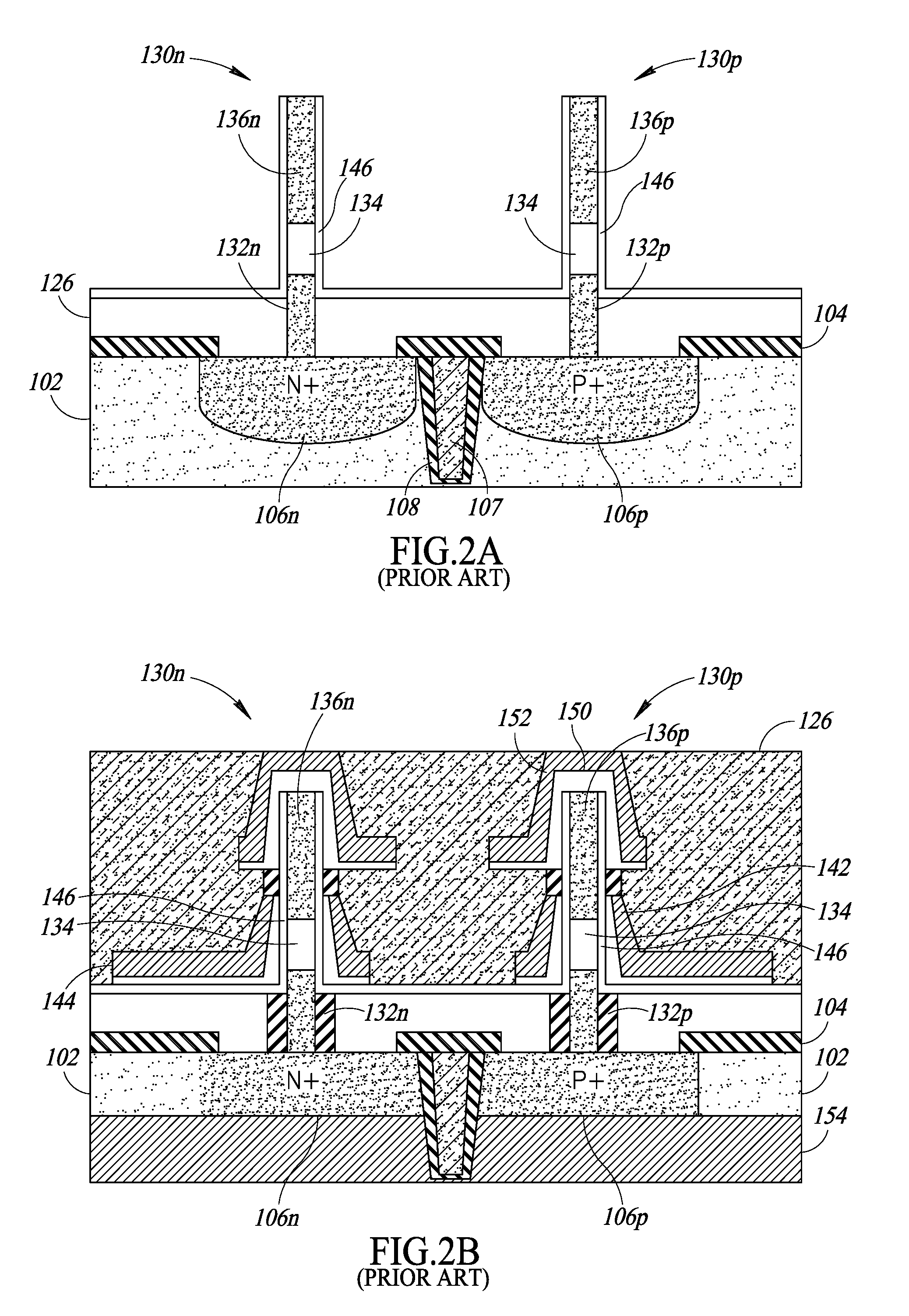
One particular challenging aspect of the vertical GAA FET stacked design is the interconnect structure.
In particular, making electrical contact to the lowest terminal of the vertical GAA FET, i.e., the source or the drain, can be awkward because the lower terminal is not accessible from the top side of the semiconductor substrate, once the vertical GAA FET is formed.

Method used


Image

  • Modular interconnects for gate-all-around transistors
  • Modular interconnects for gate-all-around transistors
  • Modular interconnects for gate-all-around transistors

Examples


Embodiment Construction

[0069]In the following description, certain specific details are set forth in order to provide a thorough understanding of various aspects of the disclosed subject matter. However, the disclosed subject matter may be practiced without these specific details. In some instances, well-known structures and methods of semiconductor processing comprising embodiments of the subject matter disclosed herein have not been described in detail to avoid obscuring the descriptions of other aspects of the present disclosure.

[0070]Unless the context requires otherwise, throughout the specification and claims that follow, the word “comprise” and variations thereof, such as “comprises” and “comprising” are to be construed in an open, inclusive sense, that is, as “including, but not limited to.”

[0071]Reference throughout the specification to “one embodiment” or “an embodiment” means that a particular feature, structure, or characteristic described in connection with the embodiment is included in at le...


PUM


Abstract

A modular interconnect structure facilitates building complex, yet compact, integrated circuits from vertical GAA FETs. The modular interconnect structure includes annular metal contacts to the transistor terminals, sectors of stacked discs extending radially outward from the vertical nanowires, and vias in the form of rods. Extension tabs mounted onto the radial sector interconnects permit signals to fan out from each transistor terminal. Adjacent interconnects are linked by linear segments. Unlike conventional integrated circuits, the modular interconnects as described herein are formed at the same time as the transistors. Vertical GAA NAND and NOR gates provide building blocks for creating all types of logic gates to carry out any desired Boolean logic function. Stacked vertical GAA FETs are made possible by the modular interconnect structure. The modular interconnect structure permits a variety of specialized vertical GAA devices to be integrated on a silicon substrate using standard CMOS processes.

Description

BACKGROUND[0001]Technical Field[0002]The present disclosure generally relates to various geometries for gate-all-around transistor devices built on a semiconductor substrate and, in particular, to vertically oriented gate-all-around transistors in which current flows in a direction transverse to the surface of the semiconductor substrate.[0003]Description of the Related Art[0004]A gate-all-around FET, or GAA FET, is a non-planar metal-oxide-semiconductor (MOS) transistor design in which the gate fully wraps around the conducting channel for maximum control of current flow therein. In the GAA FET, the channel is configured as a cylindrical nanowire that is surrounded by a gate oxide. The gate then surrounds the gate oxide.[0005]Source and drain regions are positioned on either end of the channel. Some existing GAA FETs are horizontal GAA FETs, oriented such that the nanowire extends in a horizontal direction that is substantially parallel to the surface of the semiconductor substrate...

Claims


Application Information

Patent Timeline
Patent Type & Authority Applications(United States)
IPC IPC(8): H01L27/115H01L29/423H01L27/06H01L29/08H01L23/538H01L27/02H01L29/786H01L29/66H01L29/788H01L29/06H01L27/07
CPCH01L29/42392H01L29/66742H01L29/78696H01L29/41741H01L29/517H01L29/1608H01L29/0676H01L23/5384H01L23/5386H01L29/78642H01L29/7827H01L29/775H01L29/7926H01L27/0705H01L27/092H01L27/0727H01L27/0255H01L27/0688H01L29/66439H01L21/823885H01L29/66666H01L21/823871H01L21/76895H01L21/76897B82Y40/00H10B43/27
Inventor ZHANG, JOHN H.
Owner STMICROELECTRONICS SRL
Why Eureka
Try Eureka