Microspectroscopy device

a micro-spectroscopy and device technology, applied in the direction of spectrometry/spectrophotometry/monochromators, instruments, optical radiation measurement, etc., can solve the problems of difficult direction detection, interruption of normal focusing performance, and long time-consuming maintenance of the distance between the sample and the objective lens

Active Publication Date: 2017-01-26
HITACHI HIGH-TECH CORP
View PDF2 Cites 2 Cited by
  • Summary
  • Abstract
  • Description
  • Claims
  • Application Information

AI Technical Summary

Benefits of technology

[0010]Long-term continuous analysis of large polymers such as DNA passing through a nanopore, that is, base sequence determination for e...

Problems solved by technology

Maintaining the distance between the sample and the objective lens stably for a long time at this level is difficult with only mechanical fixing, due to thermal expansion or the like.
However, at the time of long-term continuous measurement while a large biopolymer such as DNA is passing through a nanopore, p...

Method used


Image

  • Microspectroscopy device
  • Microspectroscopy device
  • Microspectroscopy device

Examples


first embodiment

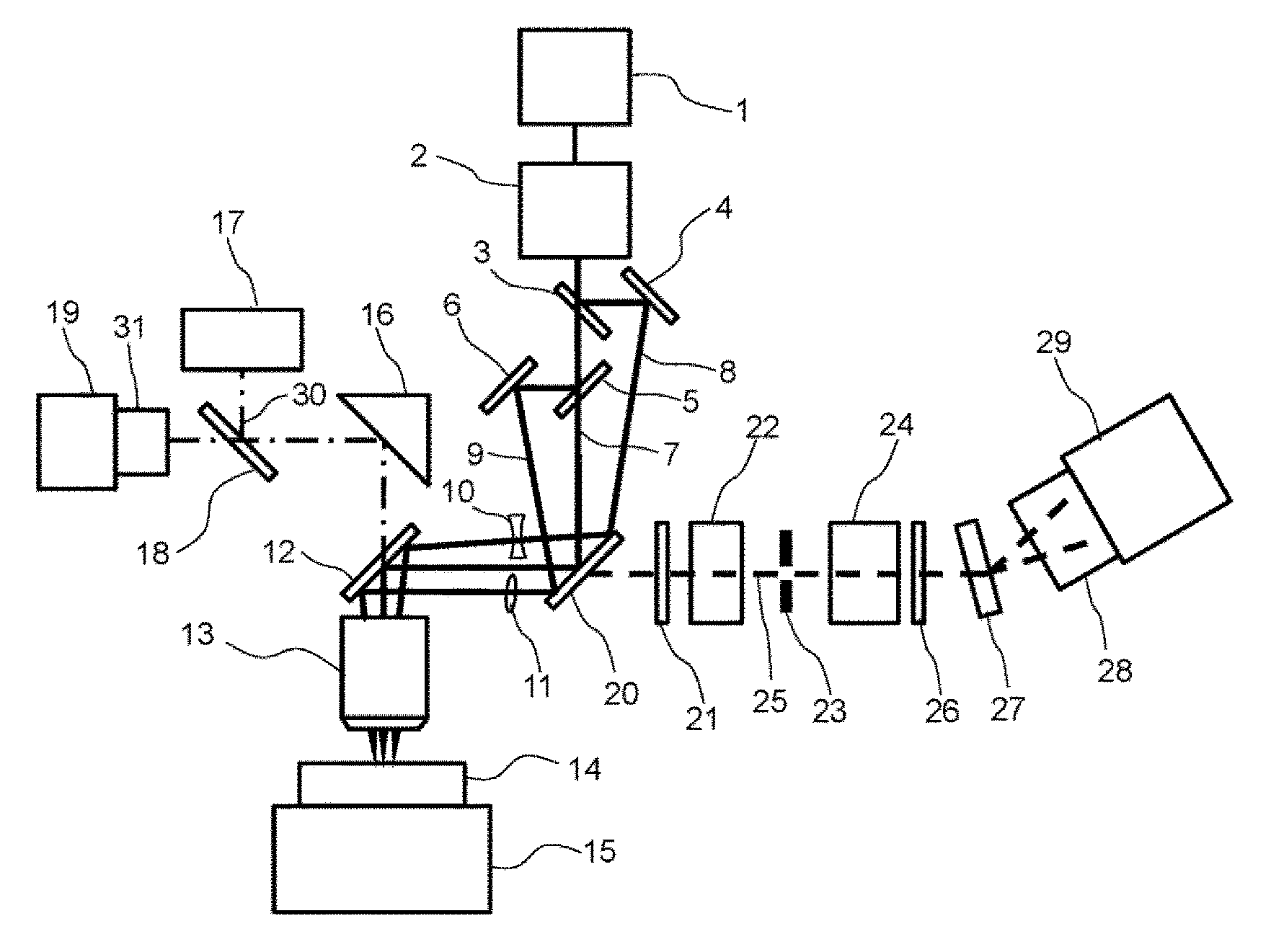
[0022]FIG. 1 is a configuration diagram showing the present invention. A beam emitted from an excitation laser light source 1 is converted into a parallel beam with a large width by a beam expander 2. The excitation laser light source 1 in this embodiment is for a near-infrared laser having a wavelength of 785 nm. The output beam of the beam expander 2 is split by beam splitters 3 and 5 into a total of three beams of a sample excitation beam 7 and defocus-sensing beams 8 and 9.

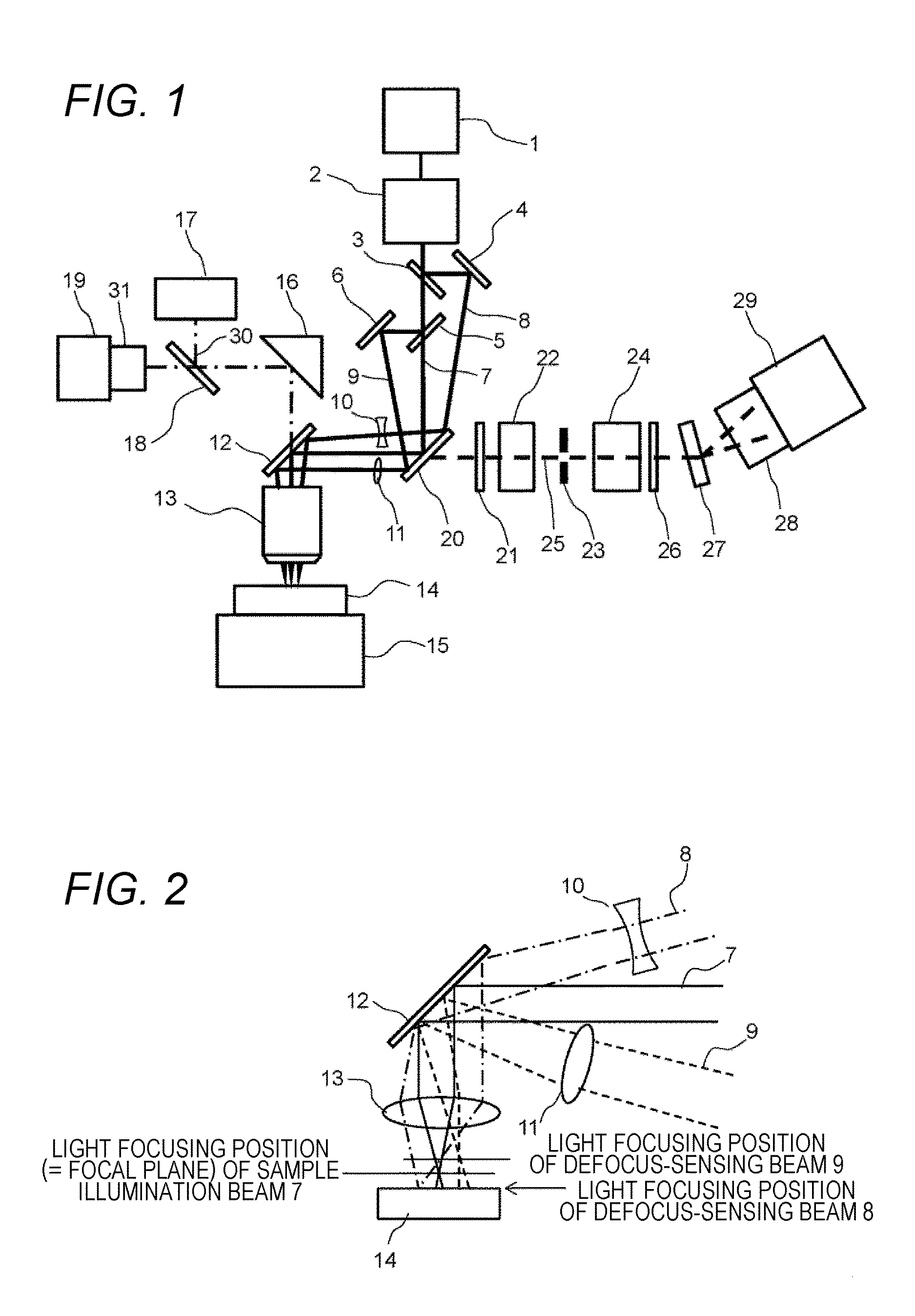
[0023]These three beams are input to an objective lens 13 by mirrors 4 and 6 and dichroic mirrors 20 and 12, and are condensed in the vicinity of the surface of a sample 14. As shown in FIG. 1, the defocus-sensing beam 8 is divided from the sample excitation beam 7 by the beam splitter 3 and is input to the objective lens 13 through the mirror 4, the dichroic mirror 20 and the dichroic mirror 12 in this order, and then is focused in the vicinity of the surface of the sample 14. Further, the defocus-sensing bea...

fourth embodiment

[0043]In the present embodiment, the excitation beam is one in number, but the excitation beam may be even multiple beams without any problems as in the

[0044]Although a diffraction beam splitter is used as a multi-beam generator in the present embodiment, a conventional beam splitter subjected to a cascade connection may be used as a matter of course.

[0045]Although embodiments of the present invention have been described mainly regarding the application to the Raman spectroscopy, the present invention can be similarly applied also to fluorescence spectroscopy.


PUM


Abstract

With a microspectroscopy device provided with an objective lens with a high numerical aperture, a defocus arises from thermal drift, etc., necessitating auto-focusing. Conventional auto-focus based on through-focus image acquisition takes time, and thus, it cannot be applied to continuous measurement over a long time wherein high-speed sampling is carried out. The present invention addresses this problem by having a defocus-sensing beam that has either defocus or astigmatism fall incident on the objective lens. Since how the image of the spot of the beam for defocus sensing blurs differs depending on the orientation of the defocus, real-time detection of the amount and orientation of defocus becomes possible, and high-speed realtime auto-focus becomes possible.

Description

TECHNICAL FIELD[0001]The present invention relates to a microspectroscopy device which is a combination of an optical microscope and a spectroscope. The present invention is useful for Raman microspectroscopy and also useful for laser induced fluorescence spectroscopy in addition. The present invention is particularly useful for applications requiring long-term continuous measurement such as determination of the DNA base sequence based on the Raman microspectroscopy, etc.BACKGROUND ART[0002]In PTL 1, a device for analyzing a biopolymer by irradiating the biopolymer passing through a nanopore with light to generate Raman scattering light, and measuring the light is described.[0003]For the analysis of the Raman scattering light, a microspectroscopy device (a combination of a microscope and a spectroscopic optical system) called a Raman microscope is used, as described in PTL 2. In a Raman microscope, in order to observe weak Raman scattering light with high sensitivity and high resolu...

Claims


Application Information

Patent Timeline
IPC IPC(8): G01J3/44G01N21/65G02B21/16G02B21/24G02B21/36G02B27/14G01J3/02G02B21/00
CPCG01J3/44G01J3/0208G01J3/021G01N21/65G02B21/16G02B21/244G02B21/365G02B27/141G02B21/0004G01N21/6458G01J3/0248G01J3/10G01J3/4406G01J3/0229G02B7/28G02B7/32G02B21/36
Inventor SONEHARA, TSUYOSHIKUSAKA, HIROMIFUJII, AKIRAYAMAMOTO, SHUHEIOOURA, TAKESHIFUJIOKA, MICHIRU
Owner HITACHI HIGH-TECH CORP
Why Eureka
Try Eureka