Method for manufacturing a bonded soi wafer and bonded soi wafer
Active Publication Date: 2017-02-02
SHIN-ETSU HANDOTAI CO LTD
View PDF16 Cites 22 Cited by
Summary
Abstract
Description
Claims
Application Information
AI Technical Summary
This helps you quickly interpret patents by identifying the three key elements:
Problems solved by technology
Method used
Benefits of technology
Benefits of technology
The patent is about a way to prevent polycrystalline silicon layers from becoming single-crystalline during the manufacturing process of a semiconductor wafer. This can occur when the layers are deposited to form a carrier trap layer, which can decrease their effectiveness. The invention proposes a method that increases the oxygen concentration at the boundary of the base wafer and the polycrystalline silicon layer, which prevents this from happening. This results in a better carrier trap layer, which is important for the performance of semiconductor devices.
Problems solved by technology
When an ordinary polycrystalline silicon layer is deposited to form a carrier trap layer, however, there has been a problem in which the polycrystalline silicon layer is annealed to occur single-crystallization depending on a thermal history during the step for manufacturing an SOI wafer or the step for manufacturing a device, and to cause to decrease the effect as a carrier trap layer.
Method used
Image
Click on the blue label to locate the original text in one second.
Reading with bidirectional positioning of images and text.
Examples
example 1
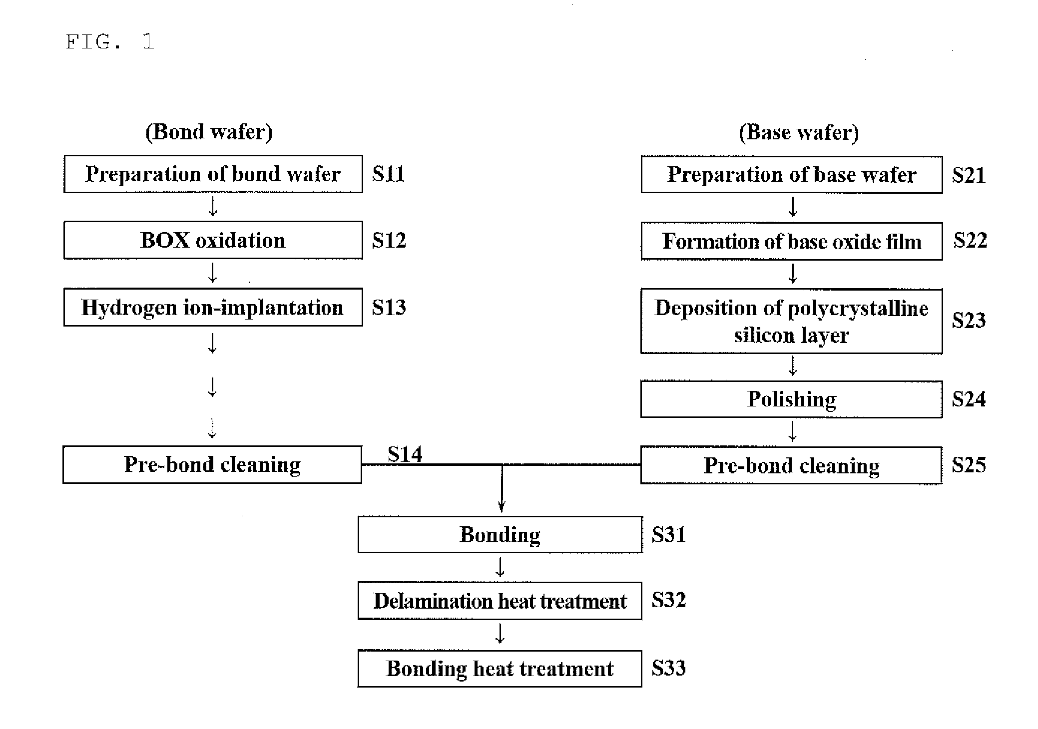
[0085]By using a manufacturing method explained in FIGS. 1 to 2, a bonded SOI wafer was produced. Provided that a p-type single crystal silicon with a diameter of 200 mm, crystal orientation of , and a resistivity of 700 Ω·cm was used as a base wafer; and formation of a base oxide film, deposition of polycrystalline silicon layer (trichlorosilane was used as a source gas), BOX oxidation, hydrogenion-implantation, a delamination heat treatment, and a bonding heat treatment were performed under the following conditions:
[0086]formation of a base oxide film: SC1+SC2 cleaning, the film thickness of an oxide film: about 1 nm
[0087]deposition of polycrystalline silicon layer: 900° C., atmospheric pressure, the film thickness: 1.0 μm (0.5 μm after polishing)
[0088]BOX oxidation: 1050° C., the film thickness of an oxide film: 400 nm
[0095]A bonded SOI wafer was produced in the same manner as in Example 1. Provided that the polycrystalline silicon layer was deposited under conditions of 920° C., atmospheric pressure, and a film thickness of 1.5 μm. (1.0 μm after polishing).
[0096]In the same manner as in Example 1, the warpage of a wafer after polishing the polycrystalline silicon layer was measured, and the state of single-crystallization of the polycrystalline silicon layer after a bonding heat treatment was examined. The results are shown in Table 1.
example 3
[0097]A bonded SOI wafer was produced in the same manner as in Example 1. Provided that the polycrystalline silicon layer was deposited under conditions of 940° C., atmospheric pressure, and a film thickness of 2.1 μm (1.6 μm after polishing).
[0098]In the same manner as in Example 1, the warpage of a wafer after polishing the polycrystalline silicon layer was measured, and the state of single-crystallization of the polycrystalline silicon layer after a bonding heat treatment was examined. The results are shown in Table 1.
PUM
Property
Measurement
Unit
Temperature
aaaaa
aaaaa
Temperature
aaaaa
aaaaa
Thickness
aaaaa
aaaaa
Abstract
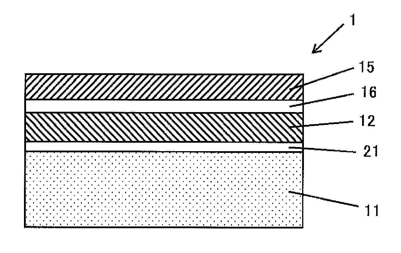
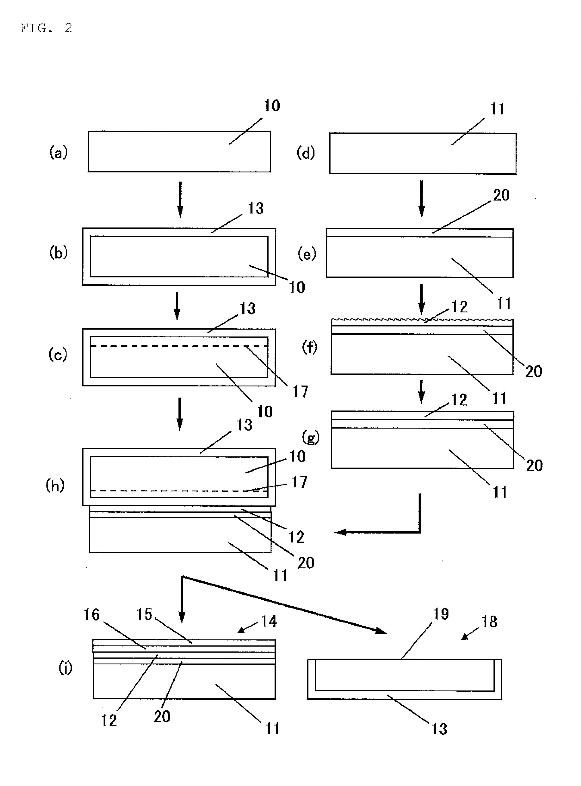
A bonded SOI wafer is manufactured by bonding a bond and a base wafer, each composed of a siliconsingle crystal, via an insulator film, depositing a polycrystalline silicon layer on the bonding surface side of the base wafer, polishing a surface of the polycrystalline silicon layer, forming the insulator film on the bonding surface of the bond wafer, bonding the polished surface of the polycrystalline silicon layer and the bond wafer via the insulator film, and thinning the bonded bond wafer to form an SOI layer; wherein, the base wafer is a siliconsingle crystal wafer having a resistivity of 100 Ω·cm or more, depositing the polycrystalline silicon layer further includes a stage for previously forming an oxide film on the surface of the base wafer on which the polycrystalline silicon layer is deposited, and the polycrystalline silicon layer is deposited at a temperature of 900° C. or more.
Description
BACKGROUND OF THE INVENTION[0001]1. Field of the Invention[0002]The present invention relates to a method for manufacturing a bonded SOI wafer and a bonded SOI wafer.[0003]2. Description of the Related Art[0004]As an SOI wafer for a RF (Radio Frequency) device, the SOI wafer has been treated by increasing the resistivity of the base wafer. However, it has been required to cope with higher frequency in order to handle further speedup, and accordingly it comes to be difficult to handle only by using conventional high-resistance wafers.[0005]As a countermeasure, it has been proposed to add a layer which is effective in annihilating generated carriers (a carrier trap layer) immediately under a buried oxide film layer (a BOX layer) of an SOI wafer. Accordingly, it is becoming necessary to form a high-resistance polycrystalline silicon layer on a base wafer to recombine carriers generated in a high-resistance wafer.[0006]Patent Literature 1 describes forming a polycrystalline silicon laye...
Claims
Application Information
Patent Timeline
Application Date:The date an application was filed.
Publication Date:The date a patent or application was officially published.
First Publication Date:The earliest publication date of a patent with the same application number.
Issue Date:Publication date of the patent grant document.
PCT Entry Date:The Entry date of PCT National Phase.
Estimated Expiry Date:The statutory expiry date of a patent right according to the Patent Law, and it is the longest term of protection that the patent right can achieve without the termination of the patent right due to other reasons(Term extension factor has been taken into account ).
Invalid Date:Actual expiry date is based on effective date or publication date of legal transaction data of invalid patent.

