Light-irradiation type thermal processing method and thermal processing apparatus

Active Publication Date: 2017-02-23
DAINIPPON SCREEN MTG CO LTD
View PDF10 Cites 13 Cited by
  • Summary
  • Abstract
  • Description
  • Claims
  • Application Information

AI Technical Summary

Benefits of technology

[0021]It is therefore an object of the present invention to measure the temperature of a front surface of

Problems solved by technology

This might become an obstacle to favorable formation of a device.
Unless the emissivity is established, temperature measurement with

Method used


Image

  • Light-irradiation type thermal processing method and thermal processing apparatus
  • Light-irradiation type thermal processing method and thermal processing apparatus
  • Light-irradiation type thermal processing method and thermal processing apparatus

Examples


Embodiment Construction

[0033]A preferred embodiment of the present invention is described in detail below by referring to the drawings.

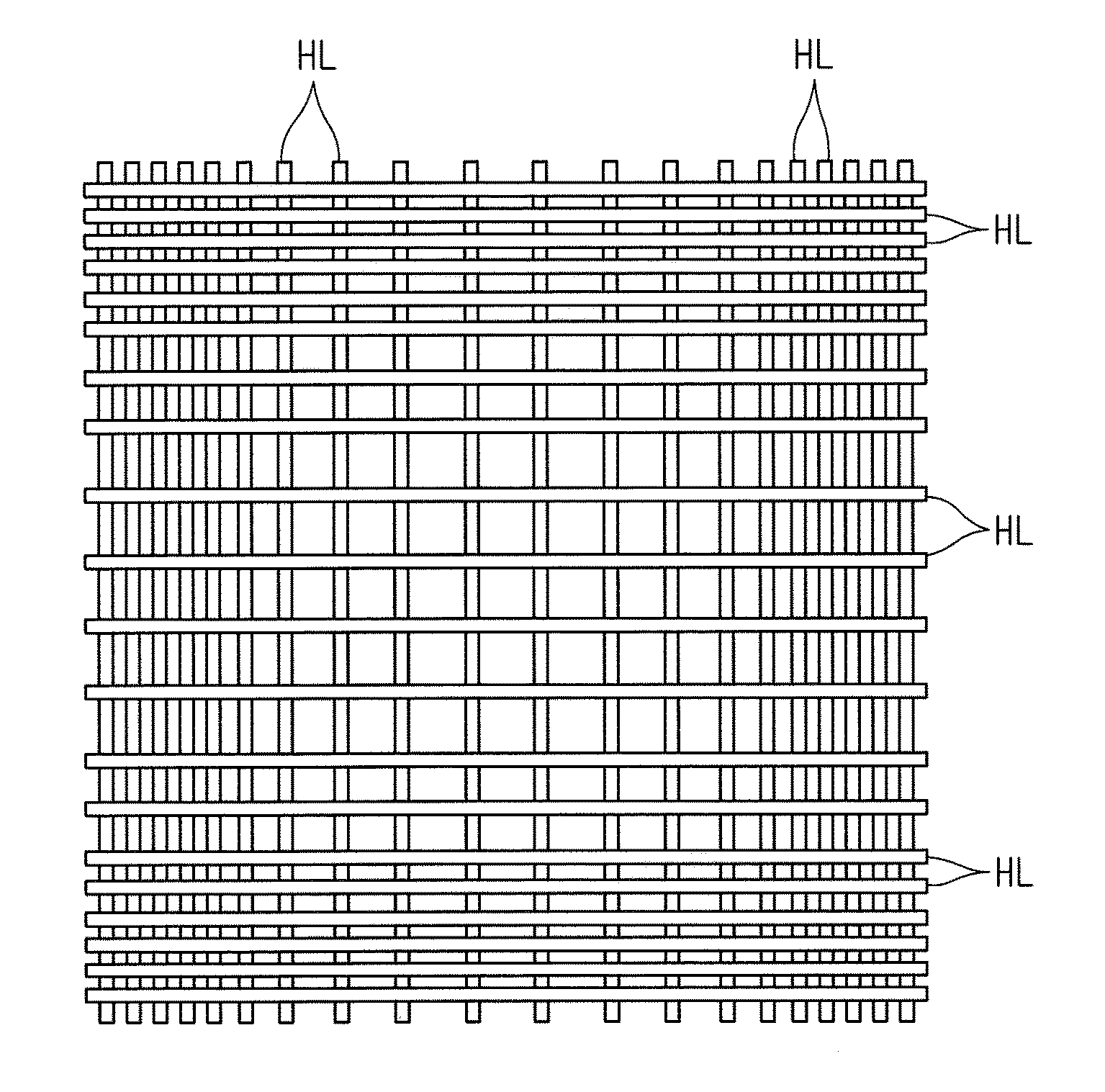
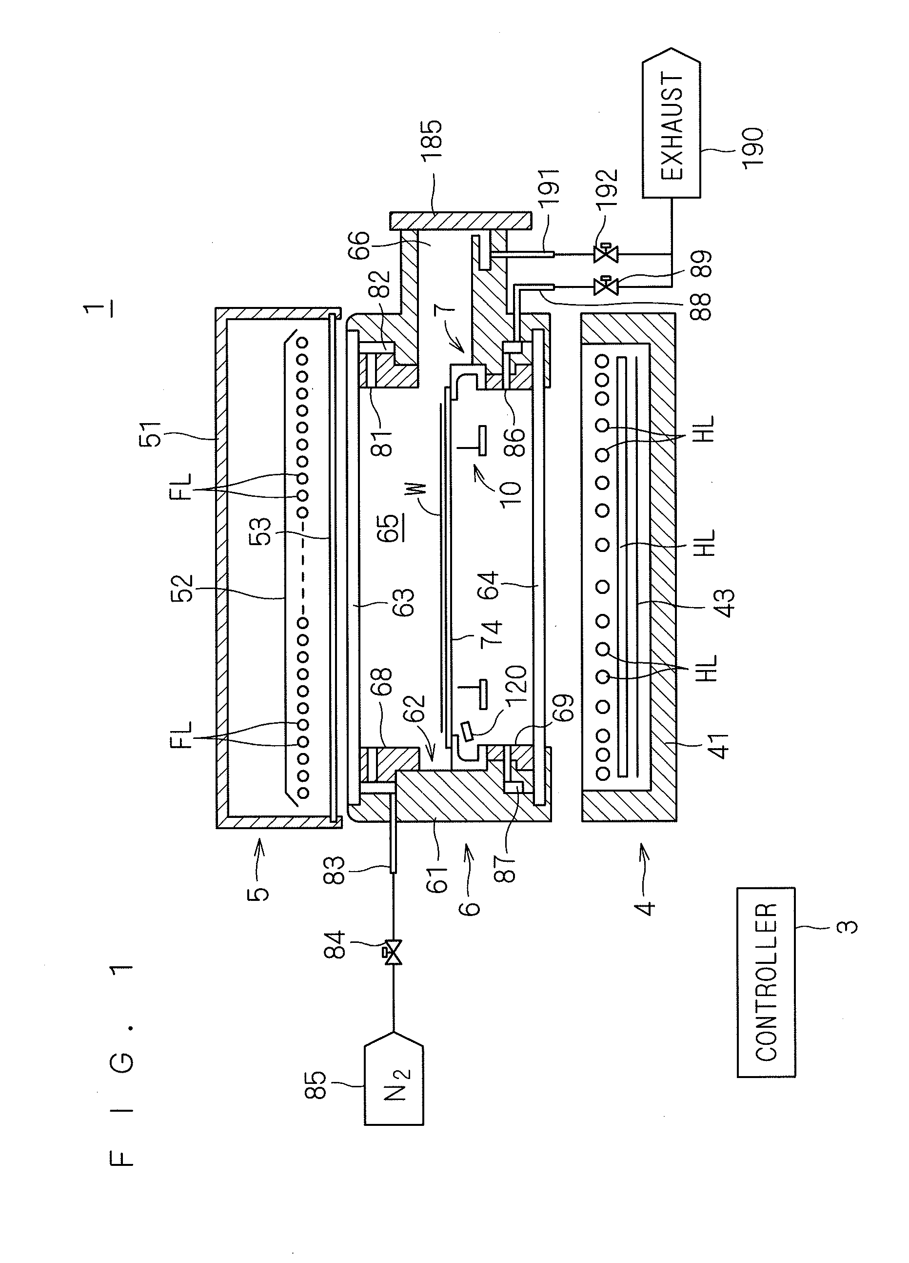
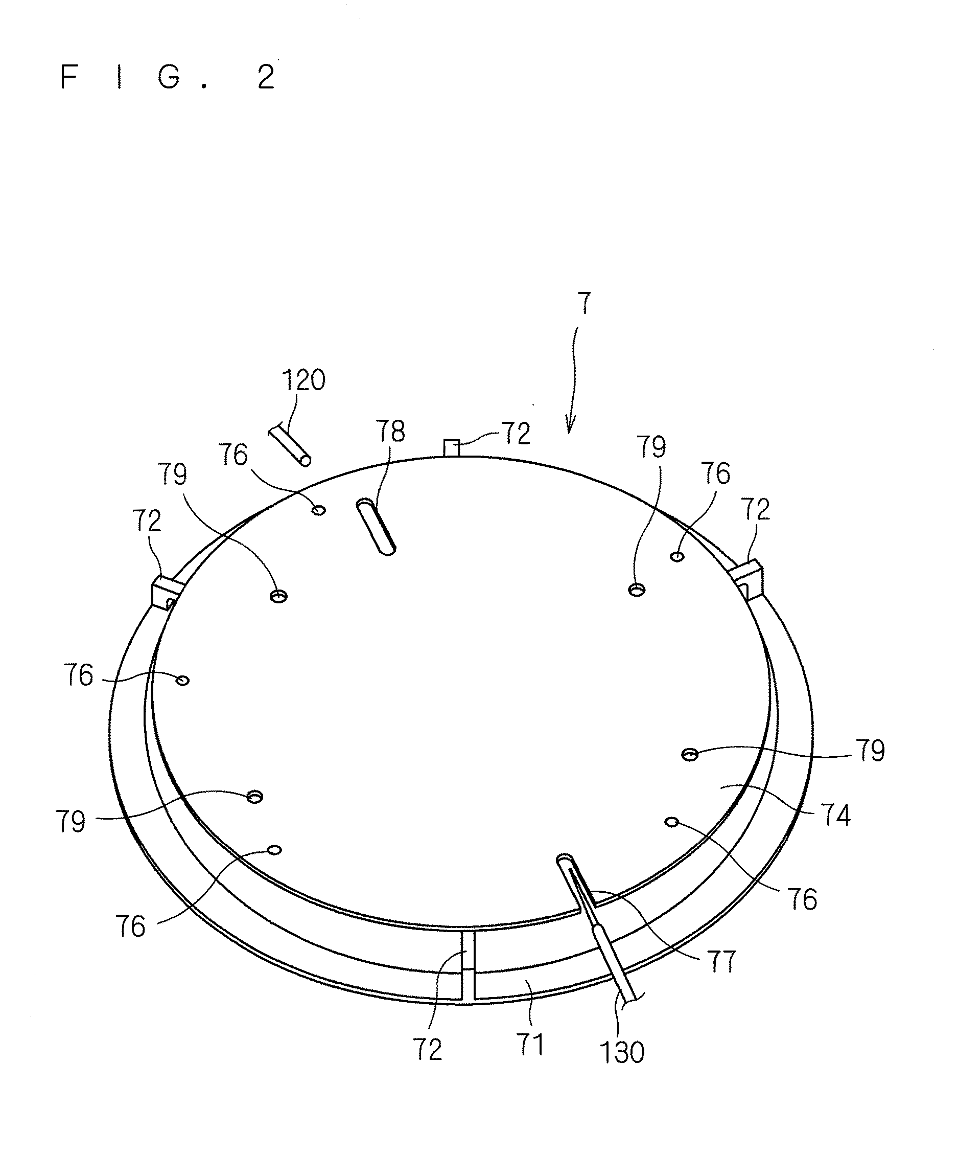
[0034]FIG. 1 is a vertical sectional view showing the structure of a thermal processing apparatus 1 according to the present invention. The thermal processing apparatus 1 of this preferred embodiment is a flash lamp annealing apparatus that heats a semiconductor wafer W of a circular plate shape as a substrate by irradiating the semiconductor wafer W with a flash. Although not specifically limited, the size of a semiconductor wafer W to be processed is 300 mm or 450 mm in diameter, for example. A semiconductor wafer W before being transported into the thermal processing apparatus 1 contains implanted impurities. The implanted impurities are activated by thermal process in the thermal processing apparatus 1. In order to facilitate understanding, in FIG. 1 and its subsequent figures, the dimensions of components and the numbers of the components are exaggerated or simplified...


PUM


Abstract

From a stage of preheating by a halogen lamp to irradiation with a flash by a flash lamp, a radiation thermometer is used for measuring the temperature of a back surface of a semiconductor wafer. A increased temperature ΔT is determined by which the back surface of the semiconductor wafer is increased in temperature from the preheating temperature by irradiation with a flash. The specific heat of the semiconductor wafer has a known value. Further, the increased temperature ΔT is proportionate to the magnitude of energy applied to a front surface of the semiconductor wafer by irradiation with a flash. Thus, a front surface attained temperature of the semiconductor wafer can be determined using the increased temperature ΔT of the back surface of the semiconductor wafer during irradiation with a flash.

Description

BACKGROUND OF THE INVENTION[0001]Field of the Invention[0002]The present invention relates to a thermal processing method and a thermal processing apparatus for heating a precision electronic substrate (hereinafter simply called a “substrate”) in the form of a thin plate such as a semiconductor wafer by irradiating the substrate with a flash.[0003]Description of the Background Art[0004]Impurity introduction performed to form a pn junction in a semiconductor wafer is an essential step in manufacturing process of a semiconductor device. At present, impurities are introduced generally by ion implantation process and subsequent annealing process. The ion implantation process is a technique of implanting impurities physically by ionizing an impurity element such as boron (B), arsenic (As), or phosphorous (P), and making the impurity ions collide with the semiconductor wafer at a highly accelerated voltage. The implanted impurities are activated by the annealing process. If the annealing ...

Claims


Application Information

Patent Timeline
IPC IPC(8): H01L21/67H01L21/66H01L21/324
CPCH01L21/67115H01L21/67248H01L22/10H01L21/324H01L21/26H01L2221/67
Inventor AOYAMA, TAKAYUKI
Owner DAINIPPON SCREEN MTG CO LTD
Why Eureka
Try Eureka