Precipitation process for producing perovskite-based solar cells

a technology of perovskite and solar cells, applied in the direction of final product manufacturing, liquid/solution decomposition chemical coating, sustainable manufacturing/processing, etc., can solve the problem of extended time for perovskite precipitation from solution, and achieve the effect of controlling the thickness of the resulting film and promoting the nucleation of perovskite crystals

Inactive Publication Date: 2017-03-23
MONASH UNIV
View PDF2 Cites 25 Cited by
  • Summary
  • Abstract
  • Description
  • Claims
  • Application Information

AI Technical Summary

Benefits of technology

[0015]In an embodiment, the method accelerates the precipitation of perovskite crystals in comparison to the case where perovskite is allowed to crystallise through the slow evaporation of the first solvent. Preferably, the step of applying the crystallisation agent results in the precipitation of the perovskite crystals within about 3 seconds of the application of the crystallisation agent. More preferably, within about 2 seconds. Even more preferably, within about 1 second. In the absence of the crystallisation agent, precipitation of perovskite from solution takes an extended period of time. This increased time for precipitation of perovskite from solution has a negative impact on the formation of the perovskite films and the efficiency of the solar cells prepared from them.
[0030]In an alternative arrangement, it is preferred that the thickness of the film is less than 1000 nm. More preferably, the thickness of the film is less than 800 nm. Even more preferably the thickness of the film is less than 600 nm. Most preferably the thickness of the film is less than 400 nm. It is advantageous to provide a thinner film as this allows for a lighter coating which reduces material usage and cost.

Problems solved by technology

In the absence of the crystallisation agent, precipitation of perovskite from solution takes an extended period of time.

Method used


Image

  • Precipitation process for producing perovskite-based solar cells
  • Precipitation process for producing perovskite-based solar cells
  • Precipitation process for producing perovskite-based solar cells

Examples


example 1

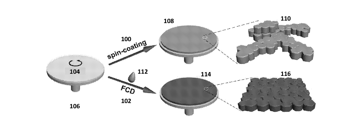
[0069]The substrates were prepared by depositing a dense TiO2 layer (30 nm thick) on fluorine-doped tin oxide (FTO) coated glass using spray pyrolysis. A DMF solution of CH3NH3PbI3 (˜45 wt %) was then spin-coated on the FTO substrate at 5000 rpm. After a short period of time (ca. 6 seconds), a solution of chlorobenzene was rapidly added and allowed to spread on the surface of the substrate. Due to the insolubility of CH3NH3PbI3, and also the two components that make up this material, in chlorobenzene, rapid nucleation and growth of the perovskite crystals occurs. An instant color change of the film from light yellow to dark brown was observed. In contrast, if no chlorobenzene was introduced, the liquid film dried more slowly during spin-coating and a shiny-grey film was obtained. The films were then subjected to annealing at 100° C. for 10 min to evaporate any residual solvent and to further promote crystallization.

[0070]FIG. 4 shows the morphology and structural characterization of...

example 2

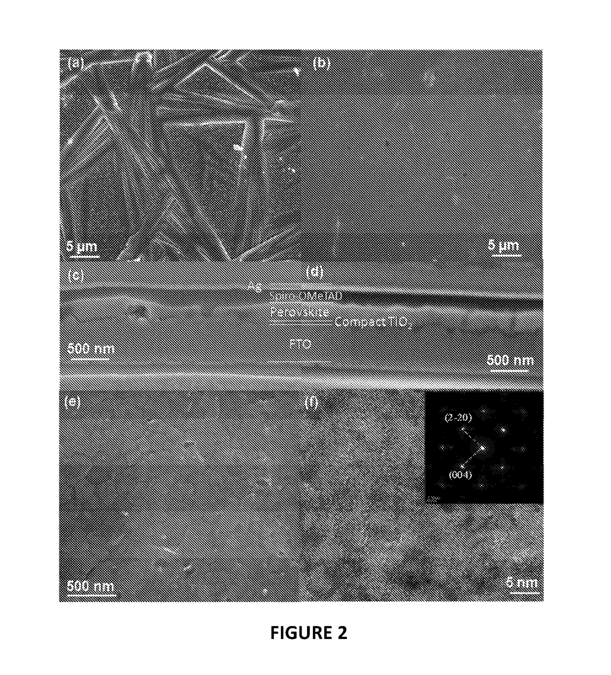
[0072]To investigate the kinetics during film formation using FCD, chlorobenzene solution was introduced onto the spinning substrate at different time to initiate the nucleation of perovskite crystal. FIG. 3 shows SEM images of the surface of the perovskite films prepared by adding chlorobenzene solution at different times. SEM images (a) and (d) show the film after 2 seconds. SEM images (b) and (e) show the film at four seconds. SEM images (c) and (f) show the film at eight seconds.

[0073]To understand the observable differences in morphology, the spin-coating process can be divided into three stages. In the first stage, the spin-off of excess solvent is a dominant process while the solution concentration remains little changed. If the chlorobenzene solution is introduced at this stage, rapid nucleation and growth of perovskite crystals happens together with solvent spin-off. Because the nucleation occurred firstly at the interface between perovskite solution and the dropped chlorob...

example 3

[0074]Solar cells were constructed with perovskite films produced by FCD using the optimized protocol.

[0075]FIG. 6 illustrates photovoltaic device characterization. a, Schematic illustration of a typical photovoltaic device. b, Cross-sectional SEM image of an optimized device. c, J-V curve of the best-performing perovskite solar cell measured at a simulated AM1.5G solar irradiation of 100 mW cm−2 (solid line) and in the dark (dashed line). d, IPCE spectrum of the solar cell corresponding to (c).

[0076]FIG. 6(a) illustrates the photovoltaic device structure. FIG. 6(b) shows a cross-sectional SEM image of an optimized photovoltaic device, taken applying focus ion beam etching. Although slight shrinkage of the spiro-OMeTAD layer was observed at the cross-section during gallium ion beam etching, which causes charging and a bright contrast at the edge of the perovskite layer, the optimized device can be clearly seen to comprise a 30-nm-thick dense TiO2 layer on FTO, a 350 nm perovskite la...


PUM

PropertyMeasurementUnit
thicknessaaaaaaaaaa
number average diameteraaaaaaaaaa
thicknessaaaaaaaaaa

Abstract

A method for the preparation of a cohesive non-porous perovskite layer on a substrate (104) comprising: forming a thin film of a solution containing a perovskite material dissolved in a solvent onto the substrate to form a liquid film (104) of the solution on the substrate, applying a crystallisation agent (112) to a surface of the film to precipitate perovskite crystals from the 5 solution to form the cohesive non-porous perovskite layer (116) on the substrate.

Description

FIELD OF THE INVENTION[0001]The present invention relates to techniques for producing perovskite films, which may be used in perovskite-based solar cells.BACKGROUND OF THE INVENTION[0002]Harvesting energy from the sun is regarded as one of the most promising ways to solve the energy issues on the earth. Developing solar cells that can efficiently covert solar energy into electricity is therefore highly desired. Although the present dominant silicon-based photovoltaic technology can achieve power conversion efficiencies (PCEs) of ˜25%, large scale applications are still limited by the high material and manufacturing costs. Great efforts have been made to develop efficient, low-cost photovoltaic technologies, including dye-sensitized solar cells, organic photovoltaic, and colloidal nanocrystal solar cells.[0003]Recently, perovskites (such as alkylammonium trihalolead(II)) have been demonstrated to be efficient photovoltaic materials due to their excellent light harvesting capabilities...

Claims


Application Information

Patent Timeline
Patent Type & Authority Applications(United States)
IPC IPC(8): H01G9/20C30B7/14C30B7/06H01L51/42C30B29/54C30B28/04H01L51/00C30B7/00C30B19/10
CPCH01G9/2009C30B7/005C30B7/14C30B7/06C30B19/106H01L2031/0344C30B28/04H01L51/0003H01L51/0028H01L51/4226H01G9/2031C30B29/54C30B29/12C30B7/00Y02E10/549C23C18/1216C23C18/1258Y02E10/542Y02P70/50H10K71/12H10K71/441H10K85/00H10K30/151H10K85/50
Inventor CHENG, YI-BINGBACH, UDOSPICCIA, LEONEHUANG, FUZHIXIAO, MANDA
Owner MONASH UNIV
Why Eureka
Try Eureka