In-situ plasma cleaning of process chamber electrostatic elements having varied geometries

a technology of electrostatic elements and process chambers, which is applied in the direction of basic electric elements, electrical equipment, electric discharge tubes, etc., can solve the problems of increased likelihood of particulate contamination on the wafer, increased dc potentials during operation, and high maintenance costs, so as to facilitate targeted etching and shorten the time

Inactive Publication Date: 2017-03-30
VARIAN SEMICON EQUIP ASSOC INC
View PDF4 Cites 8 Cited by
  • Summary
  • Abstract
  • Description
  • Claims
  • Application Information

AI Technical Summary

Benefits of technology

[0006]In view of the foregoing, provided herein are systems and methods for in-situ plasma cleaning of ion implantation system components (e.g., ion beam optics), wherein the in-situ plasma cleaning may be performed over a short time, avoiding the need to vent and / or manually clean the ion beam optics. Moreover, provided herein are systems and methods for in-situ plasma cleaning of one or more ion beam optics having varied geometries configured to generate a concentrated electric field, wherein a plasma is locally generated in an area corresponding to the concentrated electric field to facilitate targeted etching to just those surfaces in need of cleaning. By providing custom-shaped ion beam optics, plasma density is strategically enhanced in areas where surface contamination is most prevalent, thus improving cleaning efficiency and minimizing tool down time (TDT).

Problems solved by technology

These residues build up on the beam-line components, causing spikes in the DC potentials during operation (e.g., in the case of electrically biased components).
Eventually the residues flake off, causing an increased likelihood of particulate contamination on the wafer.
Accordingly, these maintenance processes may be very time consuming.
In addition, the beam-line component is not used during the maintenance processes.
As such, frequent maintenance processes may decrease the time available for IC production, thus increasing overall manufacturing cost.

Method used


Image

  • In-situ plasma cleaning of process chamber electrostatic elements having varied geometries
  • In-situ plasma cleaning of process chamber electrostatic elements having varied geometries
  • In-situ plasma cleaning of process chamber electrostatic elements having varied geometries

Examples


Embodiment Construction

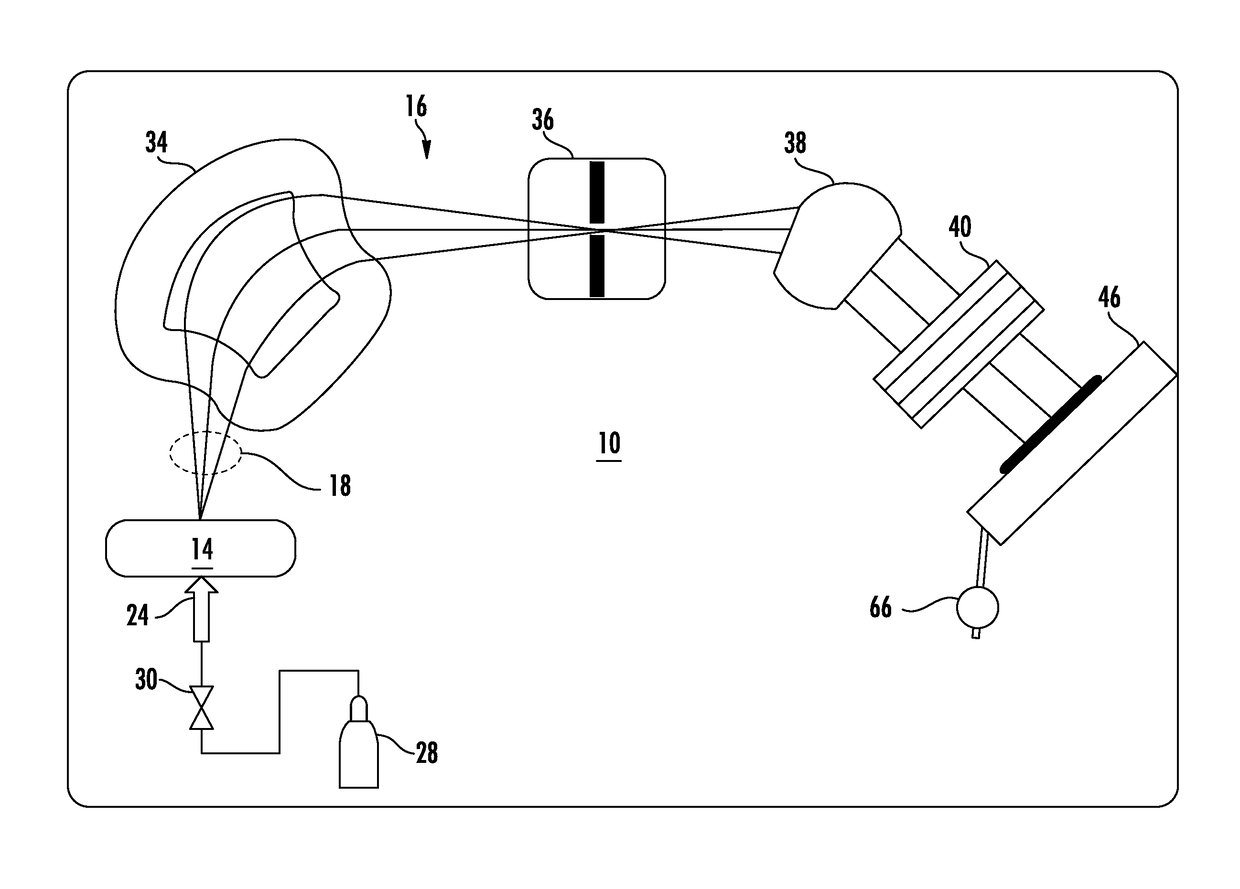
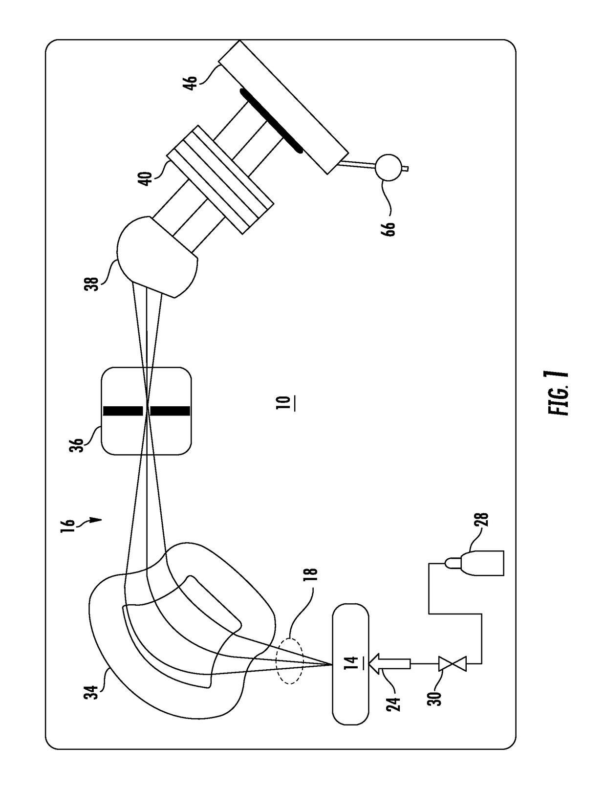
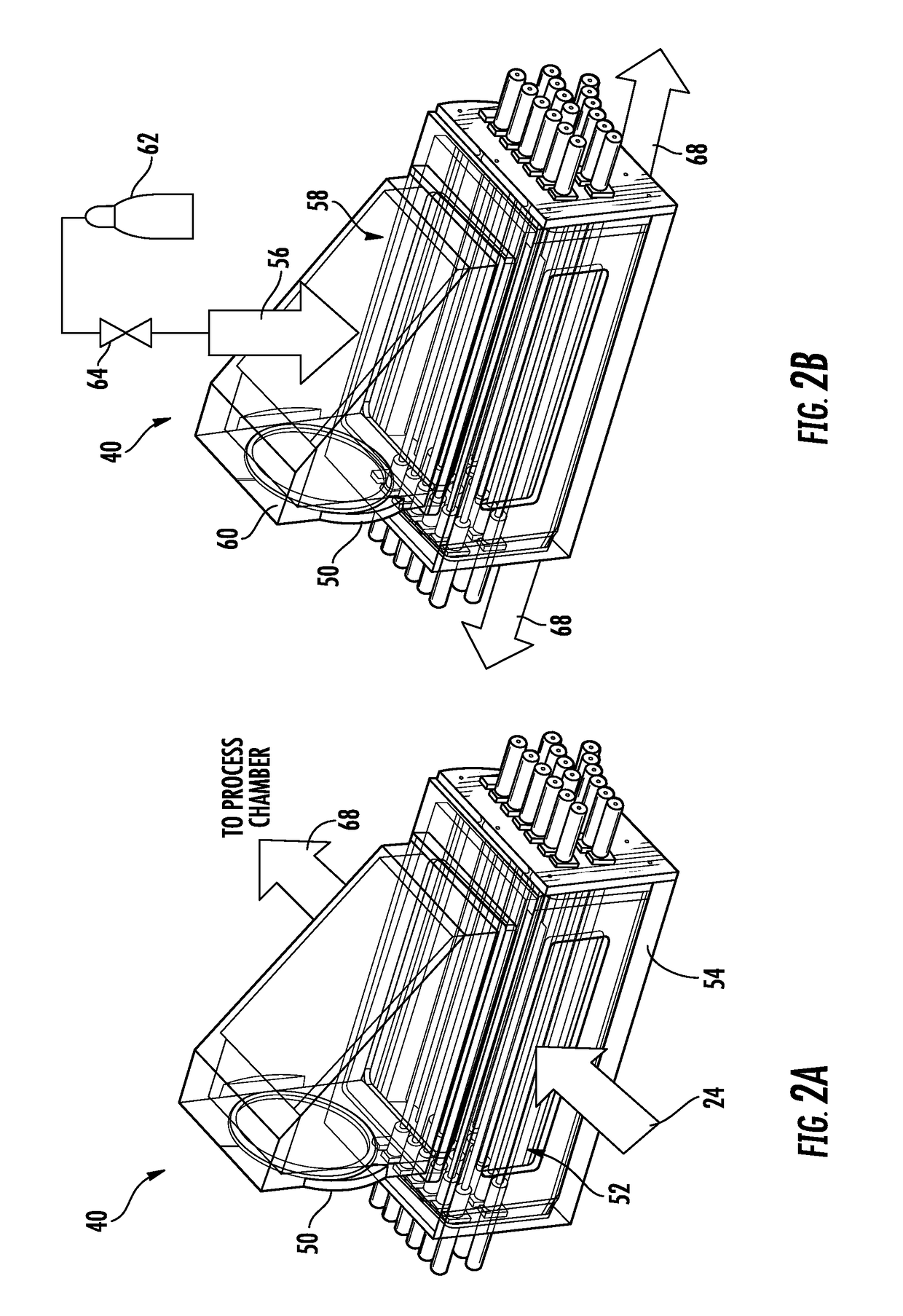
[0019]A system and method in accordance with the present disclosure will now be described more fully hereinafter with reference to the accompanying drawings, where embodiments of the system and method are shown. The system and method may be embodied in many different forms and are not be construed as being limited to the embodiments set forth herein. Instead, these embodiments are provided so this disclosure will be thorough and complete, and will fully convey the scope of the system and method to those skilled in the art.

[0020]For the sake of convenience and clarity, terms such as “top,”“bottom,”“upper,”“lower,”“vertical,”“horizontal,”“lateral,” and “longitudinal” will be used herein to describe the relative placement and orientation of these components and their constituent parts, with respect to the geometry and orientation of a component of a semiconductor manufacturing device as appearing in the figures. The terminology will include the words specifically mentioned, derivatives...


PUM


Abstract

Provided herein are approaches for in-situ plasma cleaning of one or more components of an ion implantation system. In one approach, the component may include a beam-line component having a conductive beam optic, the beam optic having a varied geometry configured to generate a concentrated electric field proximate the beam optic. The system further includes a power supply for supplying a first voltage and first current to the component during a processing mode and a second voltage and second current to the component during a cleaning mode. The second voltage and current may be applied to the one or more beam optics, in parallel, to selectively (e.g., individually) generate plasma in an area corresponding to the concentrated electric field. By providing custom-shaped ion beam optics, plasma density is strategically enhanced in areas where surface contamination is most prevalent, thus improving cleaning efficiency and minimizing tool down time.

Description

FIELD OF THE DISCLOSURE[0001]The disclosure relates generally to techniques for manufacturing electronic devices, and more particularly, to techniques for improving the performance and extending the lifetime of components within a processing chamber.BACKGROUND OF THE DISCLOSURE[0002]Ion implantation is a process of introducing dopants or impurities into a substrate via bombardment. In semiconductor manufacturing, the dopants are introduced to alter electrical, optical, or mechanical properties. For example, dopants may be introduced into an intrinsic semiconductor substrate to alter the type and level of conductivity of the substrate. In manufacturing an integrated circuit (IC), a precise doping profile provides improved IC performance. To achieve a particular doping profile, one or more dopants may be implanted in the form of ions in various doses and various energy levels.[0003]Ion implantation systems may comprise an ion source and a series of beam-line components. The ion source...

Claims


Application Information

Patent Timeline
Patent Type & Authority Applications(United States)
IPC IPC(8): H01J37/32H01L21/265H01L21/67H01J37/317
CPCH01J37/32862H01J37/3171H01J37/32889H01L21/265H01L21/67069H01J2237/335H01J2237/006H01J2237/022H01J2237/303H01J2237/31705H01L21/67034
Inventor LEE, WILLIAM DAVISANGLIN, KEVINKURUNCZI, PETERDOWNEY, RYANSCHEUER, JAY T.LIKHANSKII, ALEXANDRE
Owner VARIAN SEMICON EQUIP ASSOC INC
Why Eureka
Try Eureka