
Method for manufacturing amoled backplane and structure thereof

a backplane and active matrix technology, applied in the field of display technology, can solve the problems of mura, low manufacturing efficiency, high cost, complex process, etc., and achieve the effect of reducing the number of masks used, improving manufacturing efficiency, and simple process

Active Publication Date: 2017-05-18
SHENZHEN CHINA STAR OPTOELECTRONICS TECH CO LTD
View PDF10 Cites 4 Cited by
  • Summary
  • Abstract
  • Description
  • Claims
  • Application Information

AI Technical Summary

Benefits of technology

The present invention provides a method for manufacturing an AMOLED backplane with a simple process, reduced number of masks used, increased manufacturing efficiency, and saved costs. The method includes a solid phase crystallization process to convert amorphous silicon into poly-silicon to prevent mura on a display device caused by excimer laser annealing. The resulting AMOLED backplane structure has a simple structure, is easy to manufacture, and has a low cost. Therefore, the technical effects of the present invention are to simplify the manufacturing process, improve manufacturing efficiency, and save costs for the production of AMOLED display devices.

Problems solved by technology

The above-described process requires nine masks and thus, the process is complicated and has a low manufacturing efficiency and high cost.
Further, excimer laser annealing may induce an issue of mura on a display device.

Method used


Image

  • Method for manufacturing amoled backplane and structure thereof
  • Method for manufacturing amoled backplane and structure thereof
  • Method for manufacturing amoled backplane and structure thereof

Examples


Embodiment Construction

[0070]To further expound the technical solution adopted in the present invention and the advantages thereof, a detailed description is given to a preferred embodiment of the present invention and the attached drawings.

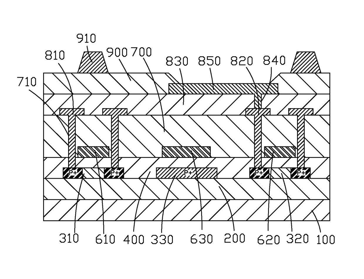
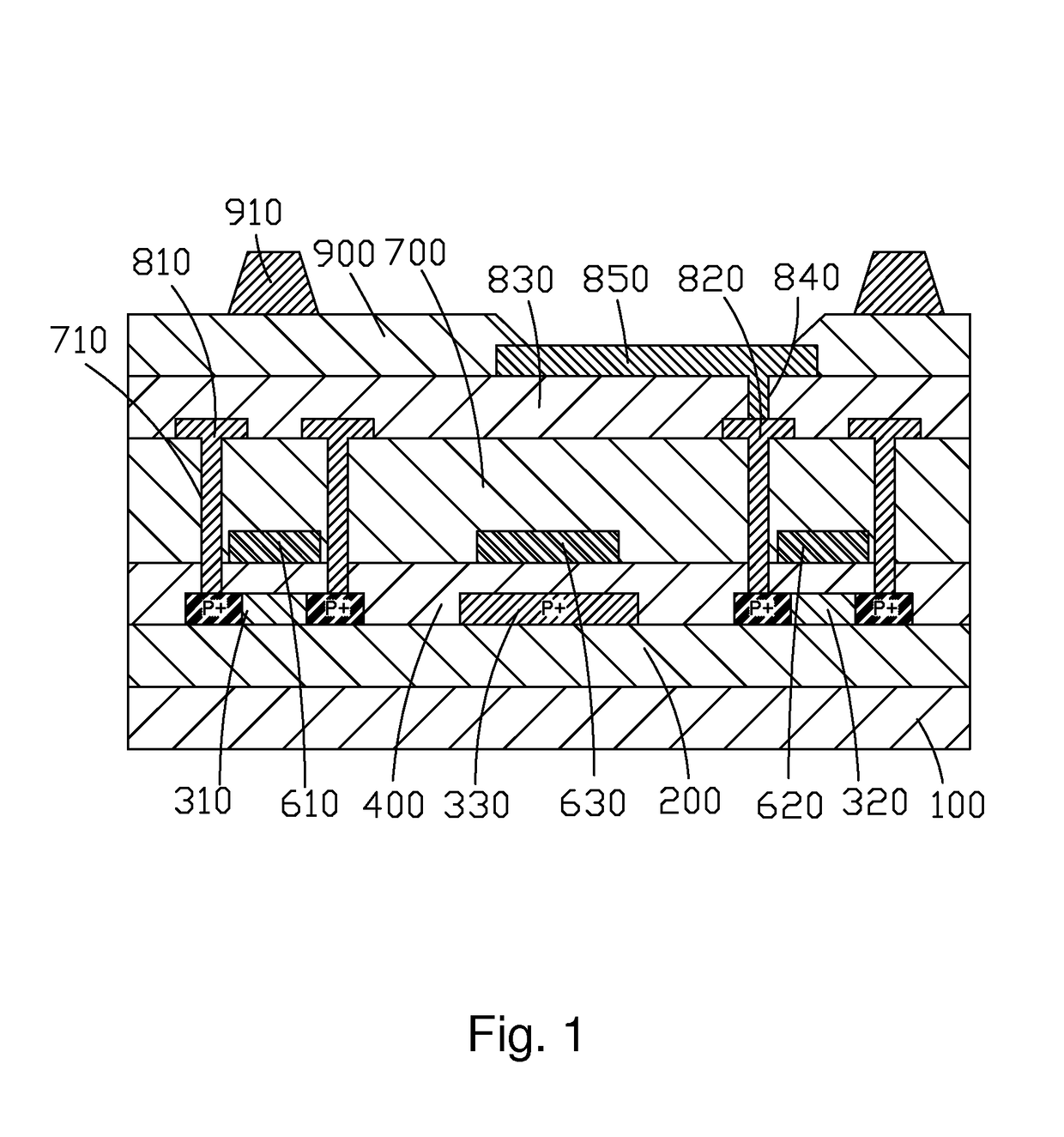
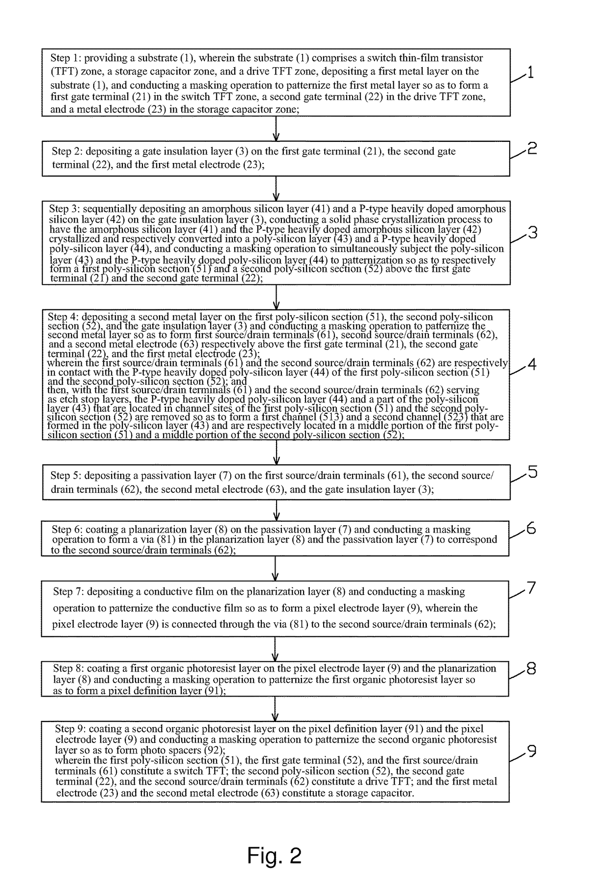
[0071]Referring to FIG. 2, the present invention provides a method for manufacturing an active matrix organic light emitting diode (AMOLED) backplane, which comprises the following steps:

[0072]Step 1: as shown in FIG. 3, providing a substrate 1, wherein the substrate 1 comprises a switch thin-film transistor (TFT) zone, a storage capacitor zone, and a drive TFT zone, depositing a first metal layer on the substrate 1, and conducting a masking operation to patternize the first metal layer so as to form a first gate terminal 21 in the switch TFT zone, a second gate terminal 22 in the drive TFT zone, and a metal electrode 23 in the storage capacitor zone.

[0073]Specifically, the first gate terminal 21, the second gate terminal 22, and the first metal electrode 23 comprise a...


PUM


Abstract

The present invention provides a method for manufacturing an AMOLED backplane and a structure thereof. The method uses a solid phase crystallization process to crystallize and convert amorphous silicon into poly-silicon so as to prevent the issue of mura on a display device caused by excimer laser annealing and adopts a back channel etching structure to effectively reduce the number of masks used. The method for manufacturing the AMOLED backplane according to the present invention needs only seven masking operations and, compared to the prior art, saves two masking operations, thereby simplifying the manufacturing process, improving the manufacturing efficiency, and saving costs.

Description

BACKGROUND OF THE INVENTION[0001]1. Field of the Invention[0002]The present invention relates to the field of display technology, and in particular to a method for manufacturing an active matrix organic light emitting diode (AMOLED) backplane and a structure thereof.[0003]2. The Related Arts[0004]In the field of display technology, the flat panel display technology, including liquid crystal display (LCD) and organic light emitting diode (OLED), has gradually taken the place of cathode ray tube (CRT) displays. Among them, OLED has various advantages, including self-luminous, low drive voltage, high emission efficiency, short response time, high sharpness and contrast, approximately 180 degree view angle, wide range of operation temperature, and being capable of achieving flexible displaying and large-area full-color displaying, and is widely used in for example mobile phone screens, computer displays, and full-color televisions and are considered a display device of the most prospero...

Claims


Application Information

Patent Timeline
IPC IPC(8): H01L51/56H01L51/52H01L27/32
CPCH01L51/56H01L51/5203H01L27/3265H01L27/3262H01L27/1255H01L27/1274H01L27/1288H10K59/80517H10K59/1201H10K71/00H10K50/805H10K50/818H10K59/00H10K59/1213H10K59/1216
Inventor HSU, YUANJUN
Owner SHENZHEN CHINA STAR OPTOELECTRONICS TECH CO LTD
Learn More