High electron mobility transistor (HEMT)

Active Publication Date: 2017-06-22
KK TOSHIBA
View PDF0 Cites 11 Cited by
  • Summary
  • Abstract
  • Description
  • Claims
  • Application Information

AI Technical Summary

Benefits of technology

[0014]In one embodiment, the highly resistive layer is grown in conditions such that C incorporation in the highly resistive layer is promoted while simultaneously introducing the donor-type impurity. The growth conditions include a low ratio of group V precursors to group III precursors, low temperature and pressure, and a high growth rate. In one embodiment, the highly resistive layer is grown using a ratio of group V precursors to group III precursors between 200 to 1400. In one embodiment, the highly resistive layer is grown at a pressure between 25 torr and 150 torr. In one embodiment, the highly resistive layer is grown at a temperature (measured at the wafer) between 900° C. and 1100° C. In one embodiment, the highly resistive layer is grown at a rate between 5 μm/hr and 9 μm/hr. In one embodiment, the donor-type impurity is Si and is introduced into the highly resistive layer by injecting silane (SiH4) while growing the highly resistive layer. In another embodiment, the donor-type impurity is O.
[0015]In one embodiment, the highly resistive layer is formed to have a variance of a concentration of the donor-type impurity less than 15% throughout the highly resistive lay

Problems solved by technology

However, doping GaN with C or Fe introduces defects in the material, which results in an increase in the on-resistance of the HEMT device when stressed at a high voltage.
This changing on-resistance is known as current collapse, and it is one problem hindering the widespr

Method used


Image

  • High electron mobility transistor (HEMT)
  • High electron mobility transistor (HEMT)
  • High electron mobility transistor (HEMT)

Examples


Example

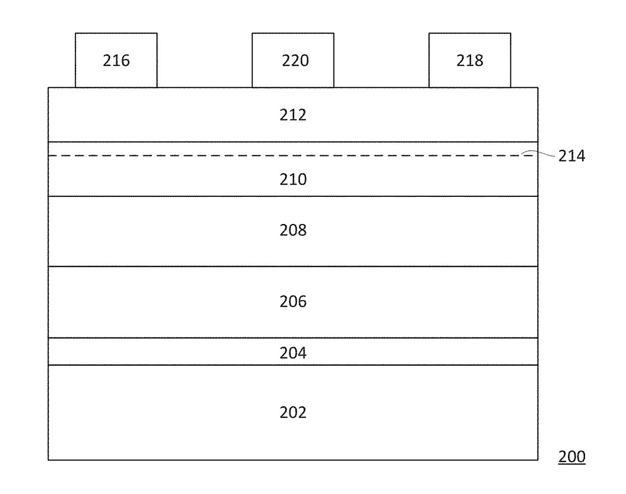
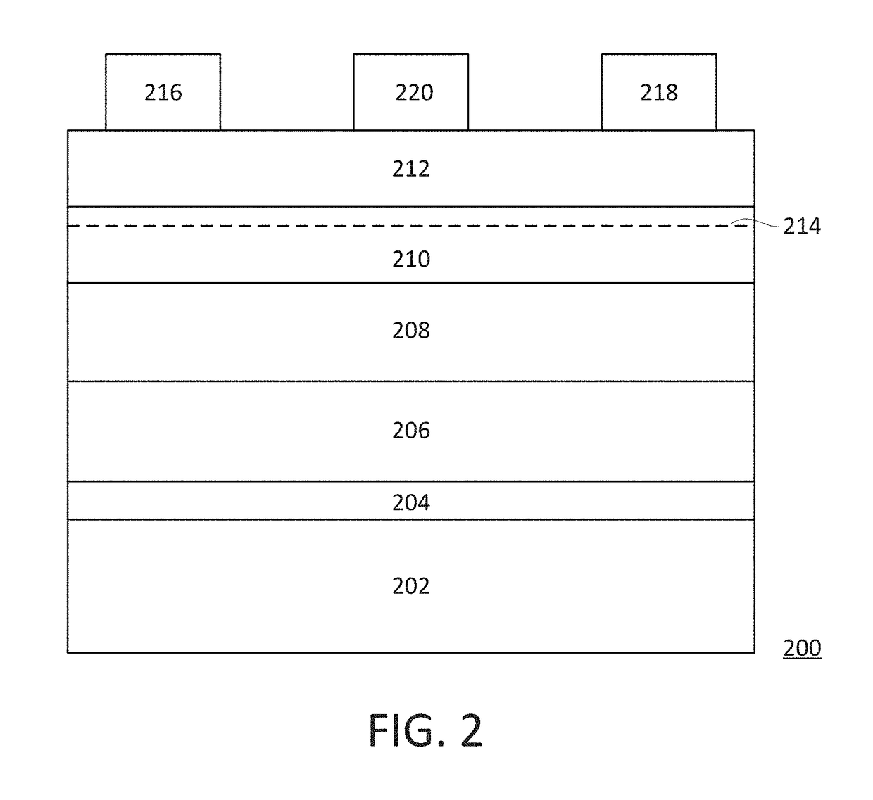
[0027]FIG. 2 shows a cross-sectional view of an HEMT device containing a highly resistive layer co-doped with C and a donor-type impurity, according to one embodiment of the invention. In FIG. 2, HEMT device 200 begins with a substrate 202. Substrate 202 can be silicon (Si), silicon carbide (SiC), sapphire (Al2O3), bulk GaN, or any other suitable substrate for epitaxially growing a group III-V material. A buffer layer 204 is formed on substrate 202 to provide a surface suitable for growing high-quality layers of group III-V materials. Buffer layer 204 can be GaN, aluminum gallium nitride (AlGaN), aluminum nitride (AlN), or any other suitable material for growing high-quality layers of group III-V materials, or combinations thereof. In one embodiment, the buffer layer 204 has a thickness between 150 Å and 40,000 Å.

[0028]A GaN layer 206 is formed on the buffer layer 204. In one embodiment, the GaN layer 206 is un-doped. The GaN layer 206 is optional (it provides a high-quality surface...


PUM


Abstract

A high electron mobility transistor (HEMT) device with a highly resistive layer co-doped with carbon (C) and a donor-type impurity and a method for making the HEMT device is disclosed. In one embodiment, the HEMT device includes a substrate, the highly resistive layer co-doped with C and the donor-type impurity formed above the substrate, a channel layer formed above the highly resistive layer, and a barrier layer formed above the channel layer. In one embodiment, the highly resistive layer comprises gallium nitride (GaN). In one embodiment, the donor-type impurity is silicon (Si). In another embodiment, the donor-type impurity is oxygen (O).

Description

FIELD OF THE INVENTION[0001]The invention relates generally to high electron mobility transistors (HEMTs), and particularly to HEMTs with a high-resistivity gallium nitride layer co-doped with carbon and a donor-type impurity.BACKGROUND OF THE INVENTION[0002]The high electron mobility transistor (HEMT) is a type of field effect transistor (FET) in which a hetero-junction between a channel layer and a barrier layer whose electron affinity is smaller than that of the channel layer. A two-dimensional electron gas (2DEG) forms in the channel layer of a group III-V HEMT device due to the mismatch in polarization field at the channel-barrier layer interface. The 2DEG has a high electron mobility that facilitates high-speed switching during device operation. In typical depletion-mode HEMT devices (also known as normally-on devices), a negatively-biased voltage may be applied to the gate electrode to deplete the 2DEG and thereby turn off the device. A group III-V HEMT device is one made of ...

Claims


Application Information

Patent Timeline
IPC IPC(8): H01L29/778H01L29/66H01L29/207H01L29/08H01L29/20H01L29/205
CPCH01L29/7787H01L29/2003H01L29/205H01L29/201H01L29/0843H01L29/66462H01L29/207H01L29/1075H01L29/7786
Inventor FENWICK, WILLIAMLEE, DONGYANG, LONG
Owner KK TOSHIBA
Why Eureka
Try Eureka