

Method of fabricating pmos devices with embedded sige
a technology of embedded sige and pmos, which is applied in the direction of semiconductor devices, basic electric elements, electrical equipment, etc., can solve the problems of high thread dislocation density of the sige layer, affecting the profile of the source/drain recess, and the defect generation of the embedded sige techniqu
- Summary
- Abstract
- Description
- Claims
- Application Information
AI Technical Summary
Benefits of technology
Problems solved by technology
Method used
Image

Examples
Embodiment Construction
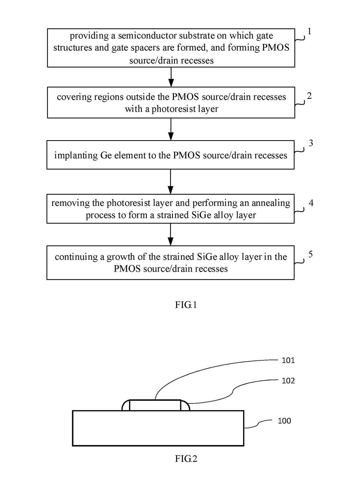
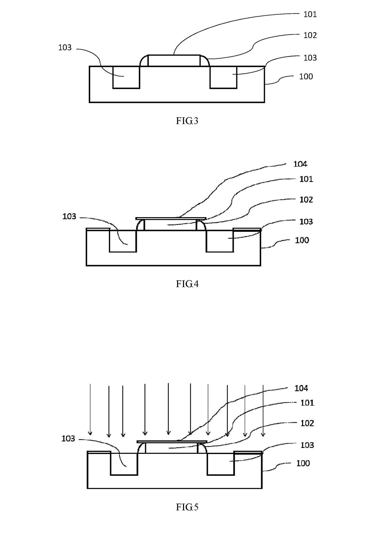
[0028]The present invention will now be descried more fully hereinafter with reference to the accompanying drawings. This invention may, however, be embodied in different forms and should not be construed as limited to the embodiments set forth herein. It will be understood by those skilled in the art that various changes in form and details may be made herein without departing from the spirit and scope of the invention.
[0029]It is noted that, in the following embodiment, the fabrication of a PMOS device with embedded SiGe is described in detail according to FIG. 2-FIG. 7. The figures referred to above are not necessarily drawn to scale, should be understood to provide a representation of particular embodiments of the invention, and should not be construed as limited to the embodiments set forth herein.
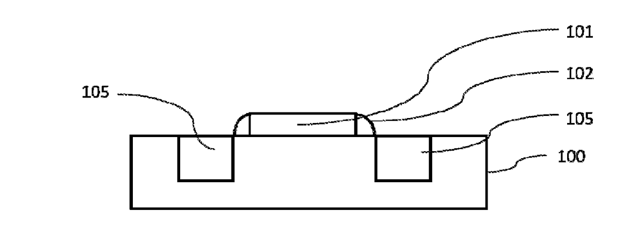
[0030]FIG. 1 is a flow chart illustrating the method of fabricating PMOS devices with embedded SiGe; FIG. 2-FIG. 7 are cross-sectional views of a PMOS devioce after each step of the m...
PUM
 Abstract
Description
Claims
Application Information