Compound for organic electronic element, organic electronic element using the same, and an electronic device thereof

Active Publication Date: 2017-08-17
DUK SAN NEOLUX
View PDF1 Cites 7 Cited by
  • Summary
  • Abstract
  • Description
  • Claims
  • Application Information

AI Technical Summary

Benefits of technology

The present invention is providing a compound that can improve the efficiency and lifespan of organic electric elements. By using this compound, organic electric elements can have higher luminous efficiency, lower driving voltage, and higher heat resistance. Additionally, they can also improve color purity and lifespan.

Problems solved by technology

The most problematic issues in an organic electric element are life span and efficiency, and the situation is such that this life span or efficiency issue must be solved as displays become larger and larger.
However, efficiency cannot be maximized only by simply improving the organic material layer.
However, since materials to be used in the hole transport layer must have low HOMO values, they mostly have low T1 values, and on account of this, the exciton formed in the light emitting layer is transferred into the hole transport layer, which causes charge unbalance in the light emitting layer and thus are emitted at a hole transport layer interface.
The light emission at the hole transport layer interface has a problem in that color purity and efficiency are lowered and life span is shortened.
However, such a stable and efficient organic material layer material for an organic electric element has not yet been fully developed.

Method used


Image

  • Compound for organic electronic element, organic electronic element using the same, and an electronic device thereof
  • Compound for organic electronic element, organic electronic element using the same, and an electronic device thereof
  • Compound for organic electronic element, organic electronic element using the same, and an electronic device thereof

Examples


synthesis example

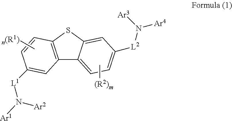
[0074]The final product represented by Formula (1) according to the present invention can be synthesized by reaction between Sub 1 and Sub 2 as illustrated in the following Reaction Scheme 1.

Synthesis Examples of Sub 1

[0075]Sub 1 of Reaction Scheme 1 can be synthesized according to, but not limited to, the reaction path of the following Reaction Scheme 2.

[0076]Examples of synthesizing specific compounds belonging to Sub 1 are as follows.

Synthesis Examples of Sub 1-1

[0077](1) Synthesis of Sub 1-1

[0078]S2-Bromo-7-chlorodibenzo[b,d]thiophene (15 g, 0.05041 mol), N-phenyldibenzo[b,d]thiophen-2-amine (13.8 g, 0.05041 mol), Pd2(dba)3 (1.38 g, 0.0015 mol), (t-Bu)3P (1.2 mL, 0.0030 mol), NaOt-Bu (14.5 g, 0.151 mol) were dissolved in anhydrous Toluene (180 mL), followed by reaction for 4 hours.

[0079]Upon completion of the reaction, the purity of the product was increased by chromatography and was carried out to obtain 20.02 g of Sub 1-1 (yield: 81%).

2. Synthesis Examples of Sub 1-5

[0080]

[008...

synthesis examples

of Sub 2

[0097]Sub 2 of Reaction Scheme 1 can be synthesized, but not limited to, the followings.

1. Synthesis Examples of Sub 2-1

[0098]

[0099]The starting material bromobenzene (40.68 g, 259.09 mmol) was dissolved in Toluene in a round bottom flask, and aniline (26.54 g, 285.00 mmol), Pd2(dba)3 (7.12 g, 7.77 mmol), 50% P(t-Bu)3 (10.1 ml, 20.73 mmol), NaOt-Bu (74.70 g, 777.28 mmol) were added to the reaction solution, followed by stirring at 80° C. Upon completion of the reaction, the reaction product was extracted with CH2Cl2 and water. The organic material layer was dried with MgSO4 and concentrated, and then the product was separated by a silicagel column and recrystallized to obtain 32.88 g of product Sub 2-1(yield: 75%).

2. Synthesis Examples of Sub 2-2

[0100]

[0101]Aniline (14.84 g, 159.30 mmol), Pd2(dba)3 (3.98 g, 4.34 mmol), 50% P(t-Bu)3 (5.6 ml, 11.59 mmol), NaOt-Bu (41.76 g, 434.47 mmol), toluene (760 ml) were added in the starting material 2-bromodibenzo[b,d]thiophene (38.11 g,...

example 1

) Manufacture and Test of Red OLED

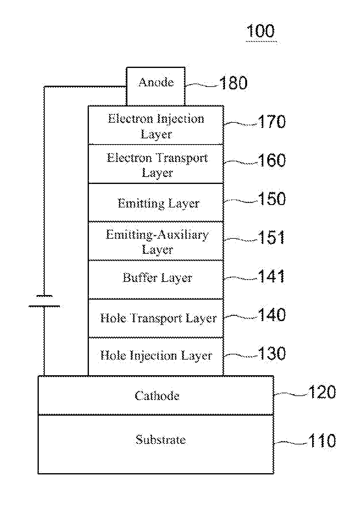
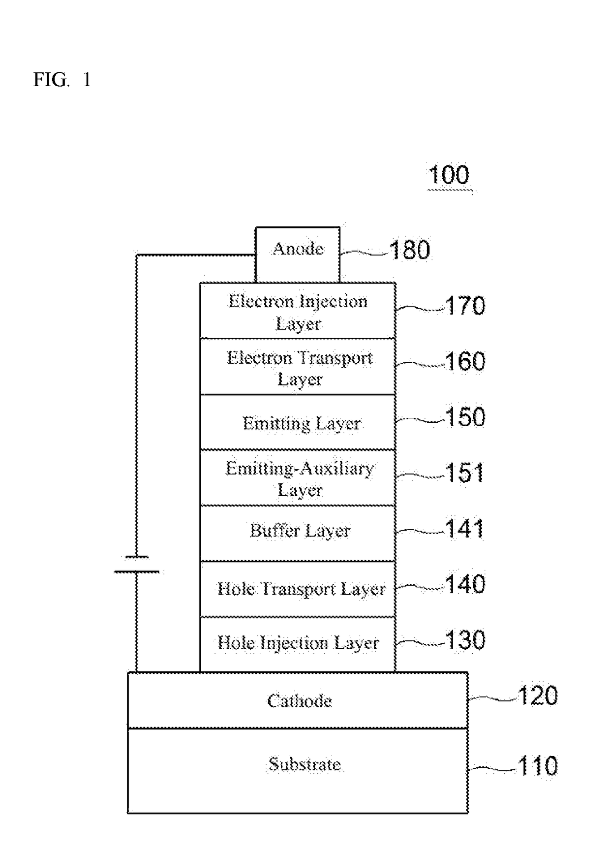
[0120]First, on an ITO layer (anode) formed on a glass substrate, N1-(naphthalen-2-yl)-N4,N4-bis(4-(naphthalen-2-yl(phenyl)amino)phenyl)-N1-phenylbenzene-1,4-diamine(hereinafter will be abbreviated as 2-TNATA) was vacuum-deposited to form a hole injection layer with a thickness of 60 nm, and N,N′-bis(1-naphthalenyl)-N,N′-bis-phenyl-(1,1′-biphenyl)-4,4′-diamine (hereinafter will be abbreviated as NPB) was vacuum-deposited to form a hole transport layer with a thickness of 60 nm. Then, the compound of the present invention represented by Formula (1) was vacuum deposited to form an emitting-auxiliary layer with a thickness of 20 nm. On the emitting-auxiliary layer, an emitting layer with a thickness of 30 nm was deposited using CBP[4,4′-N,N-dicarbazole-biphenyl] as a host doped with (piq)2Ir(acac) [bis-(1-phenylisoquinolyl)iridium(III)acetylacetonate] as a dopant in a weight ratio of 95:5. (1,1′-bisphenyl)-4-olato)bis(2-methyl-8-quinolinolato)aluminum ...


PUM


Abstract

Provided is a compound for an EBL capable of improving the light emitting efficiency, stability and life span of a device, and an organic electric element and an electronic device using the same.

Description

TECHNICAL FIELD[0001]The present invention relates to compound for organic electronic element, organic electronic element using the same, and an electronic device thereof.BACKGROUND ART[0002]In general, an organic light emitting phenomenon refers to a phenomenon in which electric energy is converted into light energy of an organic material. An organic electric element utilizing the organic light emitting phenomenon usually has a structure including an anode, a cathode, and an organic material layer interposed therebetween. Here, in many cases, the organic material layer may have a multilayered structure including multiple layers made of different materials in order to improve the efficiency and stability of an organic electric element, and for example, may include a hole injection layer, a hole transport layer, a light emitting layer, an electron transport layer, an electron injection layer, and the like.[0003]A material used as an organic material layer in an organic electric eleme...

Claims


Application Information

Patent Timeline
IPC IPC(8): H01L51/00C07D409/12C07D409/14C07D333/76C09K11/06
CPCH01L51/0061H01L51/0073C09K11/06C07D409/14C07D409/12H01L51/5088H01L51/5056H01L51/5012H01L51/0003H01L51/0005H01L51/0074H01L51/0072C09K2211/1007C09K2211/1014C09K2211/1092C09K2211/1029C09K2211/1088C07D333/76C09K2211/1011H10K85/615H10K85/622H10K85/654H10K85/6574H10K85/6576H10K85/6572H10K30/00H10K50/11H05B33/14Y02E10/549H10K85/636H10K85/324H10K50/00H10K50/15H10K50/156H10K50/17H10K71/12H10K71/135
Inventor PARK, JONG GWANGLEE, YUN SUKSO, KI HOPARK, HYOUNG KEUNJEONG, YEON SEOKPARK, JUNG HWANLEE, SUN HEELEE, GYU MIN
Owner DUK SAN NEOLUX
Why Eureka
Try Eureka