Millimeter-wave antenna device and millimeter-wave antenna array device thereof

a technology of antenna array and millimeter wave, which is applied in the direction of antennas, modular arrays, electrical devices, etc., can solve the problems of complex assembly structure, high cost, transmission loss, etc., and achieve the effect of low signal loss

Active Publication Date: 2017-08-17
NAT CHUNG SHAN INST SCI & TECH
View PDF1 Cites 15 Cited by
  • Summary
  • Abstract
  • Description
  • Claims
  • Application Information

AI Technical Summary

Benefits of technology

[0008]It is an objective of the present invention to enable a millimeter-wave antenna structure to incur low signal loss.
[0009]Another objective of the present invention is to enhance the mechanism precision of millimeter-wave antenna despite circuit-related physical size limitation.

Problems solved by technology

The aforesaid structural arrangement requires precise vertical alignment of the cavities 11 and the planar antenna elements (12, 13) to the detriment of the configuration of an RFIC die 15 of a through-silicon via (TSV) 16 and the TSV 16; as a result, not only higher costs are incurred, but, however mild, an error also leads to transmission loss.
The aforesaid assembly structure, however, is so complicated that imprecision of alignment, however mild, causes transmission loss.
The aforesaid arrangement, however, renders the spacing between the antennas overly small to the detriment of the installation of an emitting / receiving module.
The aforesaid design, however, renders it difficult to mount an emitting / receiving module.
The requirement causes antenna spacing to fall within the range of 0.6λ˜0.7λ (i.e., 4.7˜5.5 mm); as a result, the small antenna spacing leads to two problems with waveguide millimeter-wave array antenna as follows: (1) the required precision of the waveguide antenna mechanism is too strict to carry out efficient production; (2 the spacing of waveguide antennas is too small to allow an external emitting / receiving module of K-connector or waveguide flange to function.

Method used


Image

  • Millimeter-wave antenna device and millimeter-wave antenna array device thereof
  • Millimeter-wave antenna device and millimeter-wave antenna array device thereof
  • Millimeter-wave antenna device and millimeter-wave antenna array device thereof

Examples


Embodiment Construction

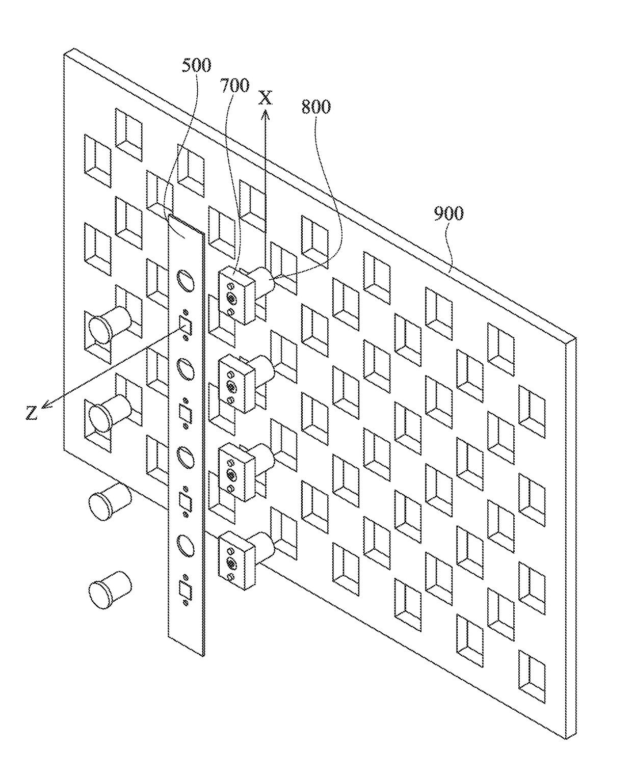
[0031]FIG. 2 is an exploded view of a millimeter-wave antenna device according to an embodiment of the present invention. FIG. 3 is a schematic view of the millimeter-wave antenna device assembled in a manner illustrated with FIG. 2 according to the embodiment of the present invention.

[0032]Referring to FIGS. 2, 3, a millimeter-wave antenna device comprises a millimeter-wave substrate 500 and coaxial cable connector bases 700. Through holes 511, 512, 521, 522 are penetratingly disposed in the millimeter-wave substrate 500 and aligned in the column direction. The millimeter-wave substrate 500 comprises a metal layer 600 and an opposing metal layer (not shown) which are disposed on and below the millimeter-wave substrate 500, respectively.

[0033]The coaxial cable connector bases 700 each have a recess 720 for holding a coaxial cable connector 800. An internal conductor 810 and an external conductor 820 of the coaxial cable connector 800 are exposed from an opening disposed at the botto...


PUM


Abstract

A millimeter-wave antenna device and a millimeter-wave antenna array device thereof are characterized in that bump portions on coaxial cable connector bases protrude into through holes of a millimeter-wave substrate to effectuate fixation thereof and ensure that the millimeter-wave substrate is tightly coupled to the coaxial cable connector bases to not only ensure the precision of the position of a feed impedance unit of a microstrip antenna structure but also ensure that, when fixed to an antenna back panel frame, a triangular configuration is effectuated such that larger antenna spacing (i.e., 8.5˜12 mm) is achieved while meeting the functional requirement of an antenna beam scan, that is, an allowance of ±30 degrees approximately, thereby circumventing a problem, i.e., the spacing between antenna units is too small to enable an external emitting / receiving module to function.

Description

FIELD OF THE INVENTION[0001]The present invention relates to antenna devices and, more particularly, to a millimeter-wave antenna device and a millimeter-wave antenna array device thereof.BACKGROUND OF THE INVENTION[0002]Millimeter-wave, also known as mm-wave for short, is electromagnetic wave with frequencies which fall between those of microwave and light wave. In general, millimeter-wave features frequencies of 30˜300 GHz and wavelengths of 1˜10 mm. Millimeter-wave provides broadband. Due to information explosion, data streams are ever-increasing in a manner that data streams beyond 4 G (B4G) will increase 1000 times by year 2020 and 10,000 times by year 2025. In view of this, the technology about the transmission of millimeter-wave is regarded as crucial to the capability of transmitting data streams at high flow rates and thus plays an important role in the development of B4G communication technology and even 5G communication technology.[0003]Referring to FIG. la, the prior art...

Claims


Application Information

Patent Timeline
Patent Type & Authority Applications(United States)
IPC IPC(8): H01Q21/00H01Q9/06
CPCH01Q9/065H01Q21/0025H01Q3/26H01Q21/064
Inventor HU, CHENG-NANLIN, DER-PHONE
Owner NAT CHUNG SHAN INST SCI & TECH
Why Eureka
Try Eureka