Large-area perovskite film and perovskite solar cell or module and fabrication method thereof

a solar cell or module technology, applied in the direction of light-sensitive devices, solid-state devices, electrolytic capacitors, etc., can solve the problems of low active material cost, high short-circuit current and high open-circuit voltage of active layer containing thin perovskite film, and achieve high-quality large-area, uniform and high-quality large-area, and reduce manufacturing time and cost

Inactive Publication Date: 2017-10-05
NAT CENT UNIV
View PDF8 Cites 32 Cited by
  • Summary
  • Abstract
  • Description
  • Claims
  • Application Information

AI Technical Summary

Benefits of technology

[0029]As mentioned above, the invention utilizes the solution process and anti-solution or Infrared light induced crystallization to rapidly fabricate the large-area perovskite film instead of using the expensive evaporation equipment, so that the manufacturing time and cost can be reduced. In addition, the method of the present invention can control the crystallization rate, crystallization level and grain size of the perovskite film based on the type of the anti-solvent, the applied speed of the anti-solvent, the film immersion time or the intensity, and time of the illumination light thereby a high-quality large-area perovskite film was obtained. Besides, the invention can further precisely control the crystallization rate, crystallization level and grain size of the perovskite film by adjusting the composition and concentration

Problems solved by technology

In the recent years the consumption of energies, especially the petrochemical and coal energies, is continuously increasing, which causes the global warming, climate change, and a lot of disasters.
Furthermore, solar cell with the active layer containing a thin perovskite film can produce high short-circuit current and high open-circuit voltage.
In addition, since the perovskite film in perovskite solar cell is very thin, s

Method used


Image

  • Large-area perovskite film and perovskite solar cell or module and fabrication method thereof
  • Large-area perovskite film and perovskite solar cell or module and fabrication method thereof
  • Large-area perovskite film and perovskite solar cell or module and fabrication method thereof

Examples


first embodiment

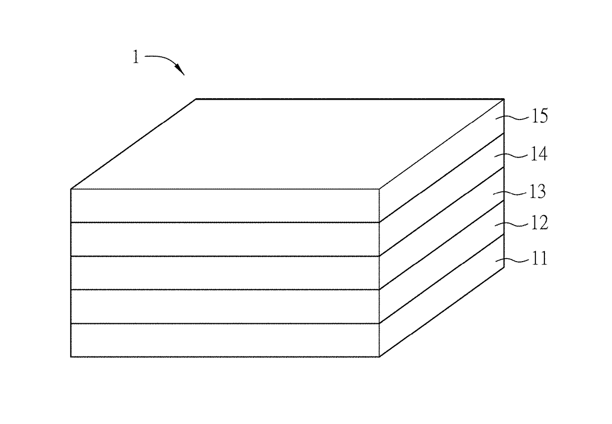
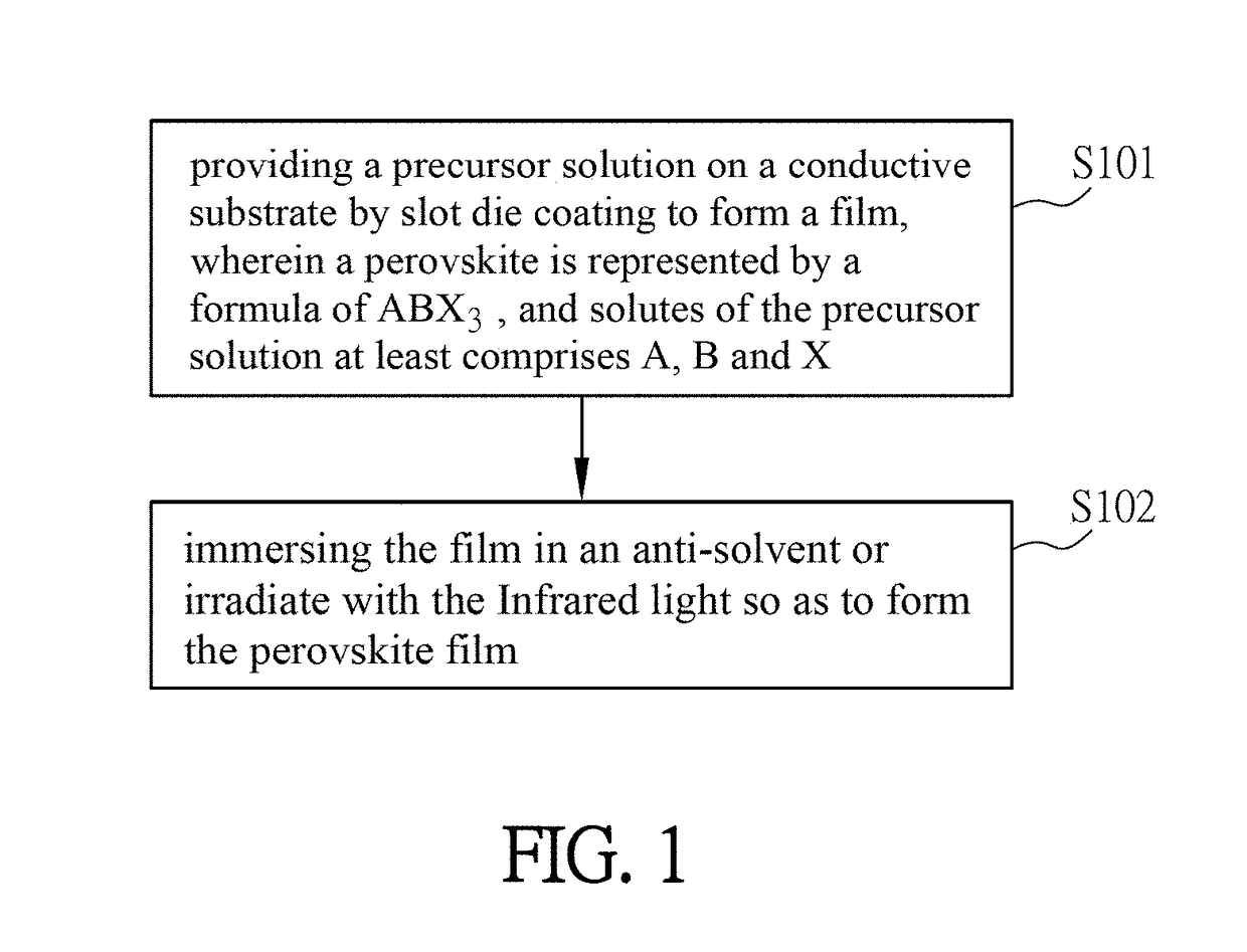
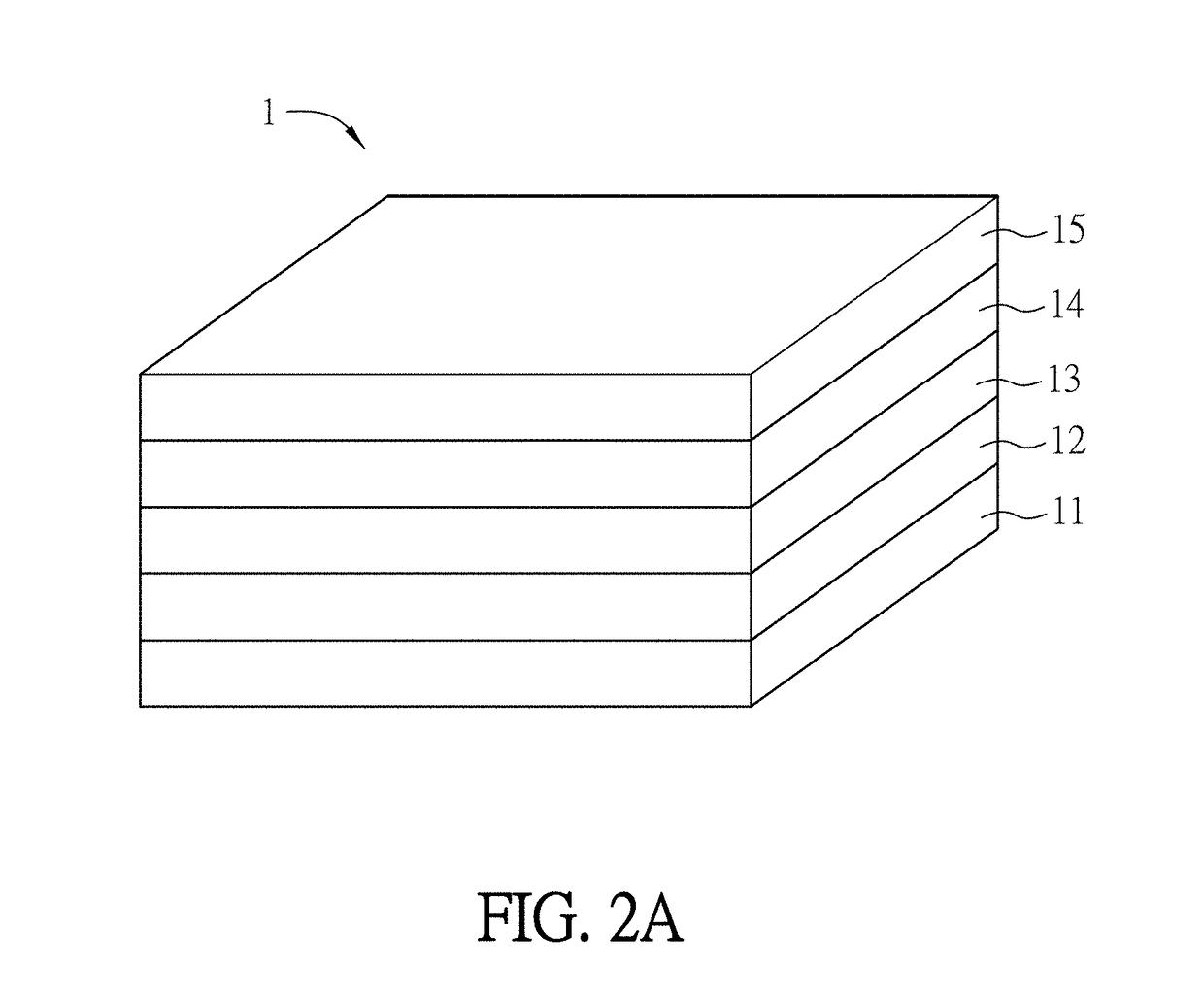
[0066]FIG. 4 is the current density vs. voltage curves of the perovskite solar module fabricated according to the invention. Referring to FIG. 4 in view of FIG. 2A, the conductive substrate 11 is an ITO / glass substrate with an area of 25 cm2, and the first carrier transporting layer 12 is made of PEDOT:PSS. CH3NH3I+PbI2 / DMF solution (30 wt %) is applied by slot die coating so as to form a film, and the film is immersed in an anti-solvent (thiophene) to form a perovskite film, thereby obtaining ITO / PEDOT:PSS / perovskite film. The perovskite film is used as the active layer 13. Then, the PCBM (30 nm) is deposited on ITO / PEDOT:PSS / perovskite to form the second carrier transporting layer 14. Finally, the silver is evaporated on the second carrier transporting layer 14 to form the electrode layer 15, thereby obtaining the perovskite solar module (6% efficiency). In addition, it is possible to adjust the concentration of the precursor solution, the coating speed, immersion conditions, and ...

second embodiment

[0068]FIG. 5 is the current density vs. voltage curves of the perovskite solar module fabricated according to the invention. Referring to FIG. 5 in view of FIG. 2A, the conductive substrate 11 is an ITO substrate, and the first carrier transporting layer 12 is made of PEDOT:PSS and deposited on the ITO substrate (100 cm2). Then, a film is formed on the ITO / PEDOT:PSS by spin coating (3000 rpm for 60 seconds) of the precursor solution (containing 0.35 M MAPbI3, 0.35 M MABr, and 0.4 M MACl in DMSO). Afterwards, at the last two seconds of spin coating of the precursor solution, the anti-solvent (iodobenzene) is applied on the spin-coated film. Then, the film is heated (annealed) at 100° C. for 30 seconds to obtain a uniform CH3NH3PbClxBryIz film. Herein, the CH3NH3PbClxBryIz film is used as the active layer 13. Then, C60 is evaporated on CH3NH3PbClxBryIz film to form the second carrier transporting layer 14. Finally, the aluminum is evaporated on the second carrier transporting layer 14...

third embodiment

[0069]FIG. 6 is the current density vs. voltage curves of the perovskite solar module fabricated according to the invention. Referring to FIG. 6 in view of FIG. 2A, the conductive substrate 11 is an ITO / PET substrate (100 cm2), and the first carrier transporting layer 12 is made of PEDOT:PSS and deposited on the ITO / PET substrate. Then, a film is formed on the ITO / PEDOT:PSS by spin coating (3000 rpm for 60 seconds) of the precursor solution (containing 0.35 M MAPbI3, 0.35 M MABr, and 0.4 M MACl in DMF). Afterwards, at the last two seconds of the spin coating the precursor solution, the anti-solvent (iodobenzene) is applied on the film. Then, the film is heated (annealed) at 100° C. for 30 seconds so as to obtain a uniform CH3NH3PbClxBryIz film. Herein, the CH3NH3PbClxBryIz film is used as the active layer 13. Then, the material C60 is evaporated on CH3NH3PbClxBryIz to form the second carrier transporting layer 14. Finally, the aluminum is evaporated on the second carrier transportin...


PUM

PropertyMeasurementUnit
Areaaaaaaaaaaa
Areaaaaaaaaaaa
Wavelengthaaaaaaaaaa

Abstract

A method of fabricating a large-area perovskite film includes steps of: providing a precursor solution on a conductive substrate to form a film, wherein the perovskite is represented by a formula of ABX3, and the solutes of the precursor solution at least comprises A, B and X; and applying an anti-solvent or Infrared light on the film. The fabrication methods of a large-area perovskite film and a perovskite solar cell or module are also disclosed.

Description

CROSS REFERENCE TO RELATED APPLICATIONS[0001]This Non-provisional application claims priority under 35 U.S.C. §119(a) on Patent Application No(s). 105110613 filed in Taiwan, Republic of China on Apr. 1, 2016, the entire contents of which are hereby incorporated by reference.BACKGROUND OF THE INVENTIONField of Invention[0002]The present invention relates to a perovskite film, a perovskite solar cell or module and fabrication method thereof. In particular, the present invention relates to a large-area perovskite film, a large-area perovskite solar cell or module and fabrication method thereof.Related Art[0003]In the recent years the consumption of energies, especially the petrochemical and coal energies, is continuously increasing, which causes the global warming, climate change, and a lot of disasters. Thus, it is desirable to develop an environmental friendly alternative energy sources. The available alternative renewable energy sources include hydraulic, wind, tidal, solar and geot...

Claims


Application Information

Patent Timeline
IPC IPC(8): H01G9/20H01L51/42H01L51/00
CPCH01G9/2009H01L51/0003H01L51/0028H01L51/0035H01L51/424H01L51/0077H01L51/0037H01L51/4213Y02E10/549Y02E10/542H10K39/10H10K71/13H10K71/441H10K85/1135H10K30/20H10K2102/103H10K85/50H10K30/10H10K71/12H10K85/30H10K85/111
Inventor WU, CHUN-GUEYCHIANG, CHIEN-HUNG
Owner NAT CENT UNIV
Why Eureka
Try Eureka