High efficiency photovoltaic cells and manufacturing thereof

a photovoltaic cell, high-efficiency technology, applied in the manufacture of final products, sustainable manufacturing/processing, electrolytic capacitors, etc., can solve the problems of reducing the conversion efficiency, not yet widely accepted as an alternative energy source solution, and the toxic nature of these materials, so as to reduce reflection

Active Publication Date: 2017-10-19
BANPIL PHOTONICS
View PDF19 Cites 5 Cited by
  • Summary
  • Abstract
  • Description
  • Claims
  • Application Information

AI Technical Summary

Benefits of technology

[0033]The present invention is expected to be found practically use in making the AR coating on any material surface to significantly reducing the reflection for the light illuminated from wide angle. By optimizing the physical parameters of the nanostructure and selection of a mat

Problems solved by technology

Although the fabrication processes of amorphous silicon based photovoltaic cells are rather simple and inexpensive, one notable downside of this type of cell is its vulnerability to defect-induced degradation that decreases its conversion efficiency.
However, due to the high cost ($3 to $5/Watt) of today's Si-based solar cell, it is not yet widely accepted as an alternative energy source solution.
This conversion efficiency is comparable to those for the single crystalline silicon photovoltaic devises; however, the toxic nature of these materials is of great concern for environment.
], which again raises issues associated with the toxic nature of these materials.
In general, synthesis processes of single crystalline group III-V are very costly because of substantial complications involved in epitaxial growth of group III-V single crystalline compound semiconductors.
], usually more than 10 times as expensive as the conventional Si-solar cell.
All photovoltaic cells in the prior art described above, regardless of what materials the cell is made from, essentially fall into one specific type of structure, which usually limits its power generation capability.
Thus, the basic structure of current photovoltaic cells ha

Method used


Image

  • High efficiency photovoltaic cells and manufacturing thereof
  • High efficiency photovoltaic cells and manufacturing thereof
  • High efficiency photovoltaic cells and manufacturing thereof

Examples


Embodiment Construction

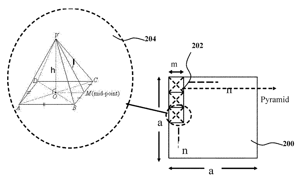
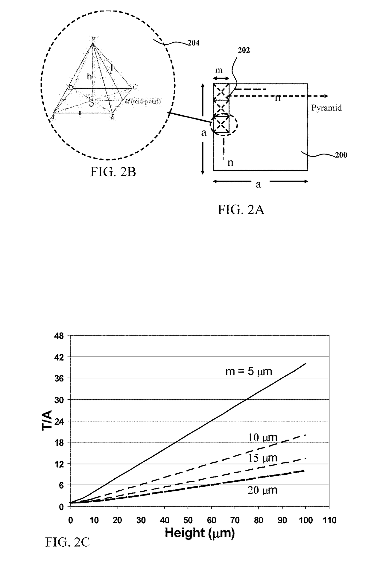
[0058]According to the present invention it is our object to provide several photovoltaic cell structures that increase the surface area, which increases the junction area, which increases conversion efficiency. Before giving the detail explanation of the photovoltaic cell structures and their manufacturing, several simulation results are first given to show the benefits of increasing the surface area.

[0059]FIGS. 2A and 2B are schematics representing the pyramid shaped structure 204 uniformly arranged on the substrate 200. FIG. 2C shows the simulation results as function of the pyramid height h, with pyramid base m as the parameter. In FIG. 2A, n number of the pyramids 204 are arranged on the axa sized substrate 200. T / A is the ratio of the surface area of the total pyramids T to the total area of axa A. It is assumed that we could make the n number of pyramids 202 on the axa-area surface. Increase of the ratio indicates the increasing increment of the surface area T as compared to ...


PUM


Abstract

This invention relates to a novel structure of photovoltaic devices (e.g. photovoltaic cells also called as solar cells) are provided. The cells are based on the micro or nano scaled structures which could not only increase the surface area but also have the capability of reducing the reflection and increasing the absorption of incident light. More specifically, the structures are based on 3D structure which are made of electric materials covering semiconductors, insulators, dielectric, polymer, and metallic type materials. By using such structures reflection loss of the light from the cell is significantly reduced, increasing the absorption, which results in increasing the conversion efficiency of the solar cell, and reducing the usage of material while increasing the flexibility of the solar cell. The structures can be also used in other optical devices wherein the reflection loss and absorption are required to enhance significantly improve the device performances.

Description

CROSS REFERENCE TO RELATED APPLICATIONS[0001]This application is a continuation-in-part of U.S. application Ser. No. 14 / 315,308 filed on Jun. 25, 2014 which is a divisional of[0002](a) U.S. patent application Ser. No. 11 / 555,445 filed on Nov. 1, 2006, now U.S. Pat. No. 8,816,191, which claims,[0003](b) The benefit and priority of U.S. Provisional Application No. 60 / 597,419 filed Nov. 29, 2005.[0004]A part of this continuous-in-part application is benefit and priority of U.S. Provisional Application No. 62 / 436,290, filed Dec. 19, 2016STATEMENT REGARDING FEDERALLY SPONSORED RESEARCH AND DEVELOPMENT[0005]New matter invention included as the continuity-in-part patent application was made with United States Government support under W91CRB11C0097 awarded by US Army Contracting Command. As such, the United States Government has certain rights in this invention.FIELD OF INVENTIONS[0006]This patent specification relates to structures of photovoltaic cells (also solar cells). More specificall...

Claims


Application Information

Patent Timeline
IPC IPC(8): H01L31/0352H01L31/0236H01L31/18H01L51/44H01L31/07H01L31/072H01G9/20H01L31/0296H01L31/0304H01L31/073H01L31/0735H01L51/42
CPCH01G9/2031H01L31/0236H01L31/0296H01L31/0304H01L31/035281H01L31/07H01L31/072H01L31/073H01L31/0735H01L31/18H01L31/1804H01L31/1828H01L31/184H01L51/4226H01L51/447Y02E10/549Y02P70/521H01L31/02327H01L31/02366H01L31/03529H10K30/87Y02E10/544Y02E10/543Y02P70/50
Inventor DUTTA, ACHYUT KUMAR
Owner BANPIL PHOTONICS
Why Eureka
Try Eureka