

Voltage balance control device and voltage balance control method for flying-capacitor multilevel converter
a multi-level converter and voltage balance control technology, applied in the direction of process control, machine control, instruments, etc., can solve the problems of difficult to control the voltage balance of the flying capacitor, the control system may erroneously judge the current direction, and the above voltage balance control method still has some drawbacks
- Summary
- Abstract
- Description
- Claims
- Application Information
AI Technical Summary
Benefits of technology
Problems solved by technology
Method used
Image

Examples
first embodiment
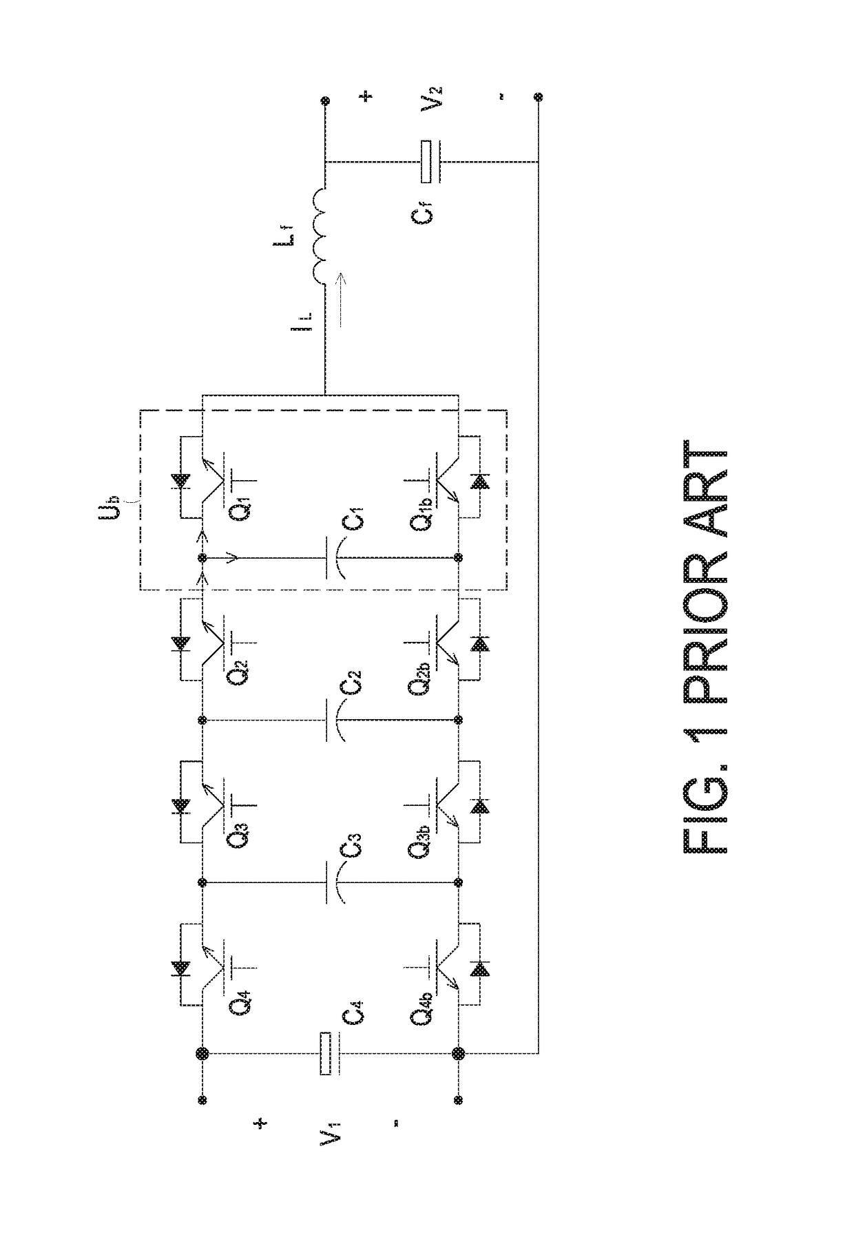
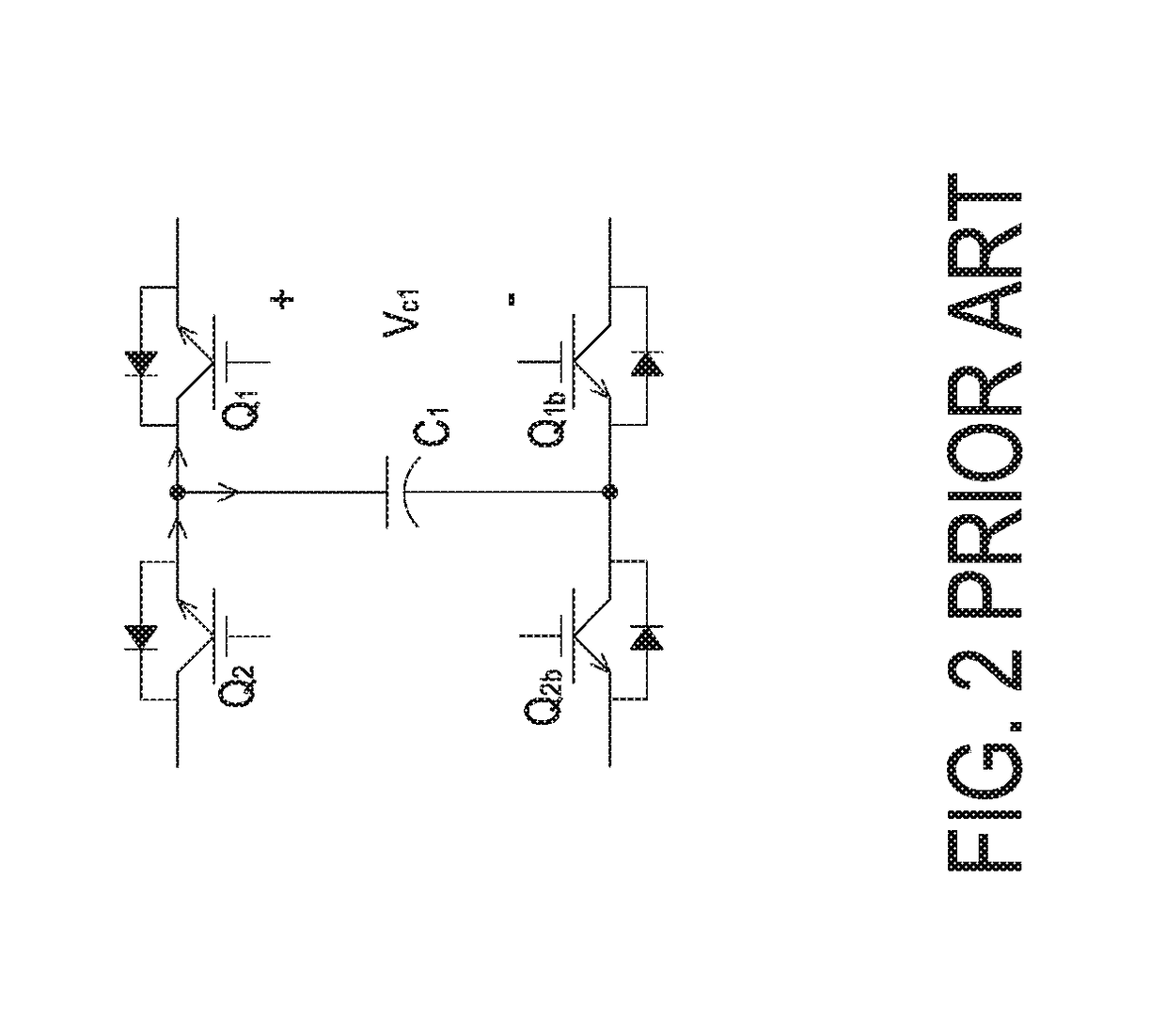
[0024]FIG. 3 is a schematic circuit diagram illustrating a voltage balance control device for a flying-capacitor multilevel converter according to the present invention. The voltage balance control device la is applied to the flying-capacitor multilevel converter 1. The flying-capacitor multilevel converter 1 comprises p basic units. That is, the flying-capacitor multilevel converter 1 comprises p flying capacitors C1, C2, . . . , Cm, . . . , Cp. Moreover, 2p semiconductor switch elements Q1, Q2, , . . . , Qm, . . . , Qp and Q1b, Q2b, . . . , Qmb, Qpb are serially connected between a positive electrode and a negative electrode of a DC voltage source, wherein m is 1, 2, . . . , (p−1). Moreover, a first end of each flying capacitor is connected with the two adjacent switching elements at a first node, and a second end of each flying capacitor is connected with the two adjacent switching elements at a second node. For example, the first end of the flying capacitor Cm is connected with ...
third embodiment
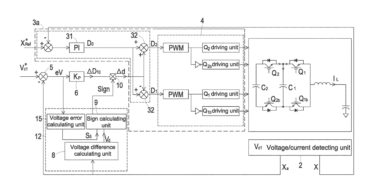
[0059]An implementation example of the voltage balance control device of the present invention will be described as follows. FIG. 7 is a schematic circuit diagram illustrating a voltage balance control device for a flying-capacitor three-level converter according to the present invention. The circuitry configuration of the voltage balance control device of this embodiment is based on the circuitry configuration of the voltage balance control device of FIG. 5. In this embodiment, the reference value XRef* indicates a given value of the output current, the second detecting result X indicates the inductor current IL, the initial duty cycle signal generator 3 of the control signal processor 3a comprises a PI regulator 31, and the duty cycle modification unit 3b of the control signal processor 3a comprises two duty cycle addition / subtraction units 32. The duty cycle modification unit 3b generates the duty cycle signals D1 and D2 corresponding to the switch elements Q1, Q1b and Q2, Q2b. T...
PUM
 Abstract
Description
Claims
Application Information