Switch device and storage unit
- Summary
- Abstract
- Description
- Claims
- Application Information
AI Technical Summary
Benefits of technology
Problems solved by technology
Method used
Image

Examples
embodiment
1. Embodiment
(1-1. Switch Device)
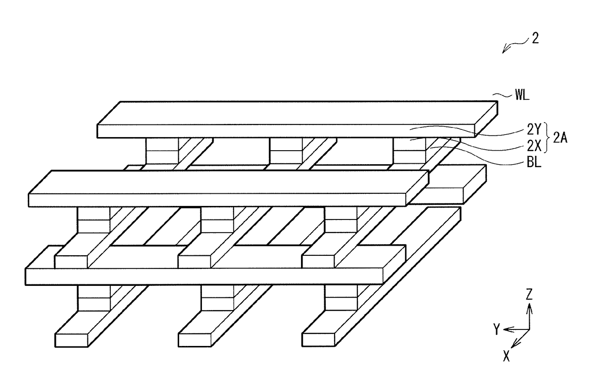
[0053]FIG. 1 illustrates a cross-sectional configuration of a switch device 1 according to an embodiment of the disclosure. The switch device 1 is provided for selectively operating any storage device (corresponding to storage device 2Y; illustrated in FIG. 3) among a plurality of storage devices in a memory cell array 2 having a so-called cross-point array structure illustrated in FIG. 3, for example. The switch device 1 (corresponding to switch device 2X; illustrated in FIG. 3) is coupled in series to the storage device 2Y (corresponding specifically to storage layer 40), and includes a lower electrode 10 (corresponding to first electrode), a switch layer 30, and an upper electrode 20 (corresponding to second electrode) in this order.
[0054]The lower electrode 10 is made of a wiring material used in a semiconductor process. Examples of the wiring material may include tungsten (W), tungsten nitride (WN), titanium nitride (TiN), copper (Cu), aluminum ...
modification example
2. Modification Example
[0084]FIG. 6A illustrates an example of a cross-sectional configuration of a switch device 3A as a modification example of the present disclosure according to the foregoing embodiment. The switch device 3A differs from the switch device 1 in that a high resistive layer 70 is provided in addition to the switch layer 30 between the lower electrode 10 and the upper electrode 20. It is to be noted that the same reference numeral is assigned to the same component in the foregoing embodiment, and description therefor is omitted.
[0085]The high resistive layer 70, for example, may have a higher insulation property than that of the switch layer 30, and may be made of, for example, an oxide or a nitride of one of a metal element and a non-metal element, or a mixture thereof.
[0086]It is to be noted that, in the switch device 3 in the present modification example, it is sufficient for the switch layer 30 and the high resistive layer 70 to be in contact with each other. In...
experiment 1
(Experiment 1)
[0090]First, the lower electrode 10 made of titanium nitride (TiN) was cleaned by means of reverse sputtering. Next, the switch layer 30 made of germanium containing nitrogen (Ge—Nx) having a film thickness of 20 nm was formed on TiN by means of reactive sputtering while allowing nitrogen to flow into a film-forming chamber, following which tungsten (W) having a film thickness of 30 nm was formed to serve as the upper electrode 20. Thereafter, a heat treatment at 320° C. for 2 hours and a pattering were performed, and then fixed resistances were coupled in series to thereby fabricate a switch device (Experimental Example 1-1, 1 Resistance to 1 Selector Device) for measurement of characteristics. Further, a switch device (Experimental Example 1-2) for measurement of characteristics including the switch layer 30 made of germanium containing oxygen (Ge-Ox) was fabricated using the similar method except allowing oxygen to flow into the film-forming chamber. Compositions of...
PUM
 Abstract
Description
Claims
Application Information
 - R&D Engineer
- R&D Manager
- IP Professional
- Industry Leading Data Capabilities
- Powerful AI technology
- Patent DNA Extraction
Browse by: Latest US Patents, China's latest patents, Technical Efficacy Thesaurus, Application Domain, Technology Topic.
© 2024 PatSnap. All rights reserved.Legal|Privacy policy|Modern Slavery Act Transparency Statement|Sitemap