Organic electroluminescent display device and method of sealing the same
a technology of electroluminescent display and organic light, which is applied in the direction of organic semiconductor devices, sustainable manufacturing/processing, and final product manufacturing, etc., can solve the problems of complex manufacturing process, long manufacturing time, and defects in organic light emitting elements, so as to reduce the spread of filling material, reduce the misalignment of the first, and easily and safely absorb moisture permeation
- Summary
- Abstract
- Description
- Claims
- Application Information
AI Technical Summary
Benefits of technology
Problems solved by technology
Method used
Image
Examples
first embodiment
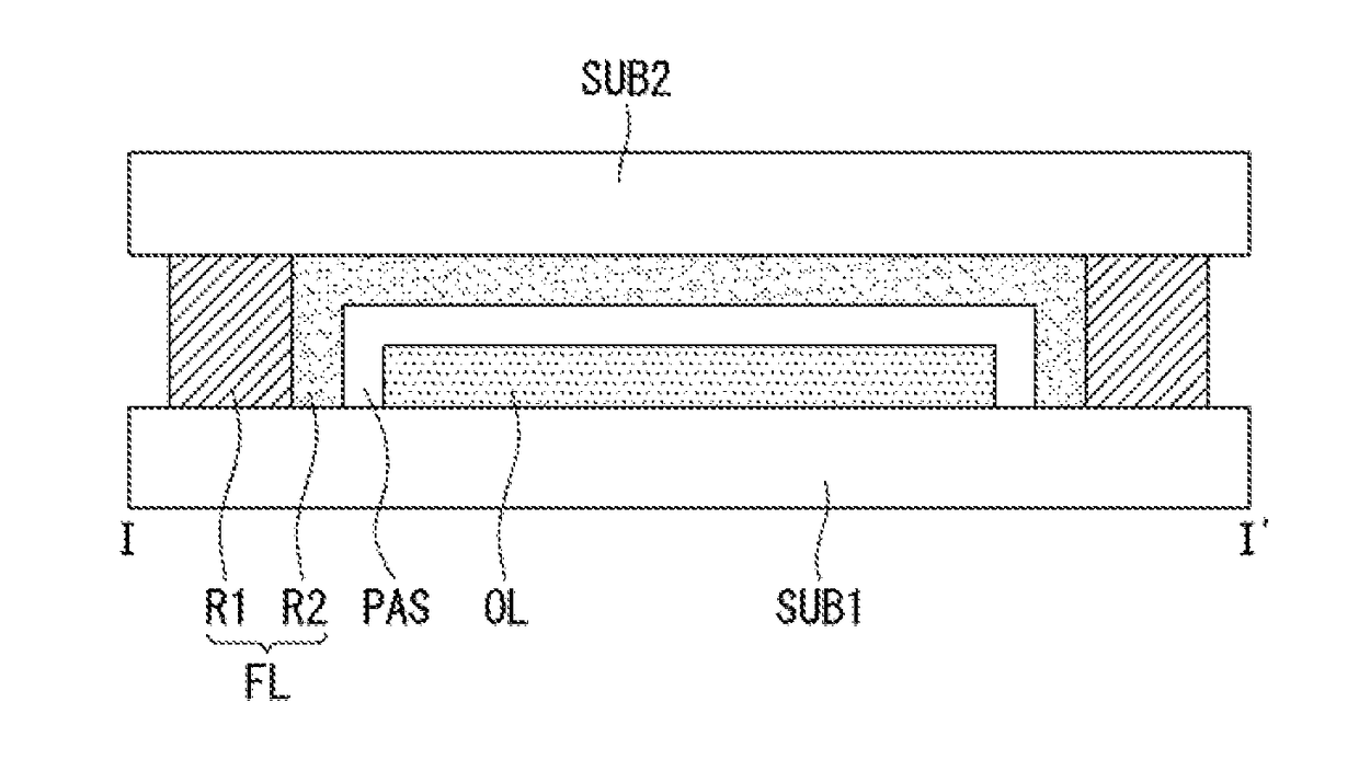
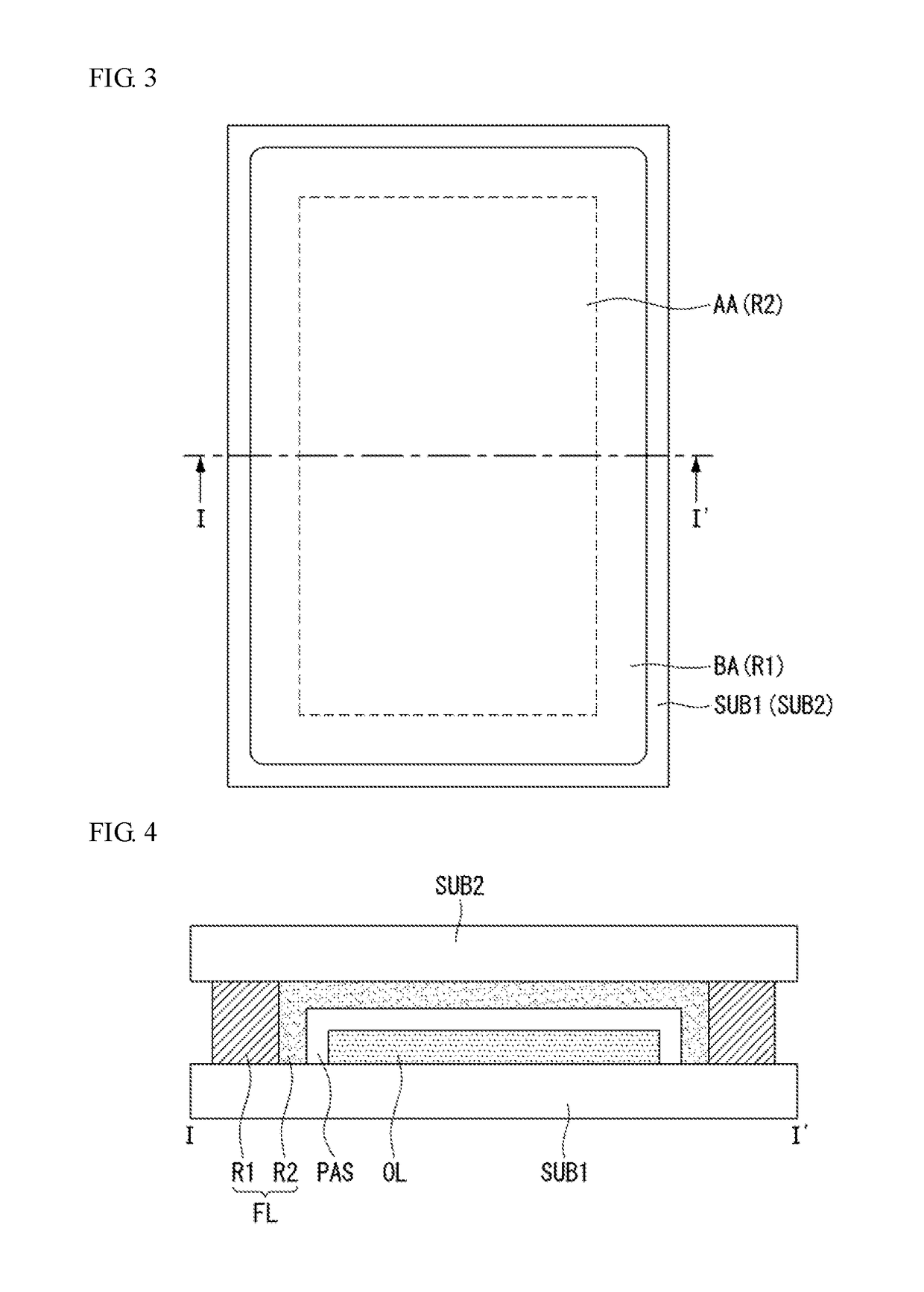
[0040]Referring to FIGS. 3 and 4, the organic electroluminescent display device according to this disclosure includes a first substrate SUB1, a second substrate SUB2, an organic light emitting element layer OL disposed on the first substrate SUB1, a passivation film PAS, and a filling layer FL.
[0041]The organic light emitting element layer OL a layer including display elements such as data lines, gate lines, thin film transistors, and organic light emitting diodes formed on the first substrate SUB1. The passivation film PAS covers the organic light emitting element layer OL to block oxygen and moisture from being penetrated into the organic light emitting element layer OL. The passivation film PAS may consist of a plurality of layers in which an inorganic protective film and an organic protective film are alternately disposed. The inorganic protective film is more suitable than the organic protective film in blocking penetration of oxygen and moisture. The organic protective film ca...
second embodiment
[0059]Referring to FIGS. 7 and 8, the organic electroluminescent display according to this disclosure includes a first substrate SUB1, an organic light emitting element layer OL and a passivation film PAS sequentially disposed on the first substrate SUB1, a second substrate SUB2, color filters CF disposed on the second substrate SUB2, a first black matrix BM1, at least one black matrix BM2 and a filling layer FL filled in a space between the first substrate SUB1 and the second substrate SUB2.
[0060]The organic light emitting element layer OL is a layer including display elements such as data lines, gate lines, thin film transistors, and organic light emitting diodes formed on the first substrate SUB1.
[0061]The passivation film PAS covers the organic light emitting element layer OL to block oxygen and moisture from being penetrated into the organic light emitting element layer OL. The passivation film PAS may consist of a plurality of layers in which an inorganic protective film and a...
PUM
 Abstract
Description
Claims
Application Information
 - R&D
- Intellectual Property
- Life Sciences
- Materials
- Tech Scout
- Unparalleled Data Quality
- Higher Quality Content
- 60% Fewer Hallucinations
Browse by: Latest US Patents, China's latest patents, Technical Efficacy Thesaurus, Application Domain, Technology Topic, Popular Technical Reports.
© 2025 PatSnap. All rights reserved.Legal|Privacy policy|Modern Slavery Act Transparency Statement|Sitemap|About US| Contact US: help@patsnap.com


