
Semiconductor manufacturing apparatus

Inactive Publication Date: 2017-12-07
SAMSUNG ELECTRONICS CO LTD
View PDF0 Cites 7 Cited by
  • Summary
  • Abstract
  • Description
  • Claims
  • Application Information

AI Technical Summary

Benefits of technology

The invention provides a semiconductor manufacturing apparatus that can produce a material layer that has good step coverage even if other process parameters vary.

Problems solved by technology

As semiconductor devices have been increasingly downscaled, it has become more difficult to conformally form thin layers.
Thus, it becomes increasingly difficult for thin layers to maintain high step coverages, and process conditions become more complicated.

Method used


Image

  • Semiconductor manufacturing apparatus
  • Semiconductor manufacturing apparatus
  • Semiconductor manufacturing apparatus

Examples


experimental example 1

[0160]A zirconium oxide (ZrO2) material layer was formed on a bare silicon substrate without a modifier by using TEMAZ as a source material and using ozone (O3) serving as an oxidizer as a reaction material.

[0161]Also, ZrO2 material layers were respectively formed by using methanol and tetrahydrofuran (THF) as modifiers according to a timing scheme shown in FIG. 5A.

[0162]In particular, after the material layer was adsorbed on a silicon substrate by supplying the modifier, a deposition rate (Å / cycle) of the material layer was calculated while varying a purge time. FIG. 8 is a graph of the deposition rate of the material layer relative to the purge time.

[0163]As a result, when methanol was used as the modifier, even if a purge time of about 400 seconds elapsed, a deposition rate of the ZrO2 material layer was not saturated. By comparison, when THF was used as the modifier, after an initial purge time of about 5 seconds elapsed, it could be confirmed that the deposition rate of the ZrO...

experimental example 2

[0165]A ZrO2 material layer was formed on a bare silicon substrate without a modifier by using TEMAZ as a source material and using ozone serving as an oxidizer as a reaction material.

[0166]Also, ZrO2 material layers were respectively formed by using methanol and THF as modifiers according to the timing scheme shown in FIG. 5A.

[0167]In particular, a deposition rate (Å / cycle) of the material layer was calculated while varying a feeding time of the modifier. FIG. 9 is a graph of the deposition rate of the material layer relative to the feeding time of the modifier.

[0168]As a result, when methanol was used as the modifier, it was confirmed that the deposition rate of the ZrO2 material layer was continuously reduced until a feeding time reached about 60 seconds. When THF was used as the modifier, the deposition rate of the ZrO2 material layer was continuously reduced for about 3 seconds. However, when a feeding time became more than 3 seconds, it was confirmed that the deposition rate o...

experimental example 3

[0170]To observe whether or not a step coverage is improved when an oxide layer is deposited using a modifier in an actual trench structure, ALD experiments were conducted by using methanol and THF as modifiers. A trench having a width of about 50 nm, a depth of about 350 nm, and an aspect ratio of about 7 was used as a target trench structure, and a ZrO2 material layer was formed by using TEMAZ as a source material and using ozone (O3) serving as an oxidizer as a reaction material.

[0171]A feeding scheme of each feed material was carried out according to the feeding scheme shown in FIG. 5A. By supplying the modifier for about 5 seconds and 400 seconds, thicknesses of formed ZrO2 material layers were measured at a top and a bottom portion of a trench.

[0172]As a result, Table 1 was obtained.

TABLE 1MethanolTHFModifier5 sec400 sec5 sec400 secfeeding timeTop of trench85 Å70 Å90 Å94 ÅBottom of79 Å49 Å83 Å89 ÅtrenchStep coverage93%70%92%95%

[0173]When methanol was used as the modifier and s...


PUM

PropertyMeasurementUnit
Fractionaaaaaaaaaa
Fractionaaaaaaaaaa
Fractionaaaaaaaaaa

Abstract

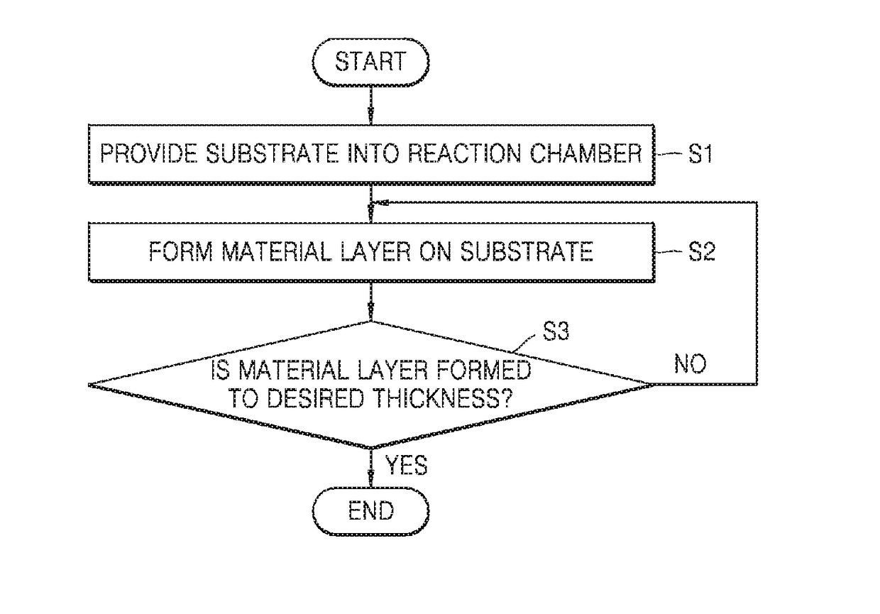
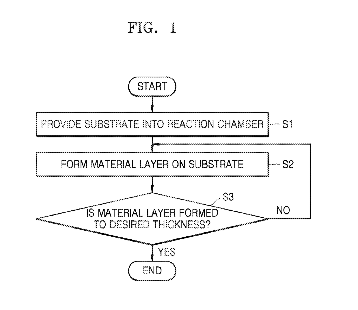
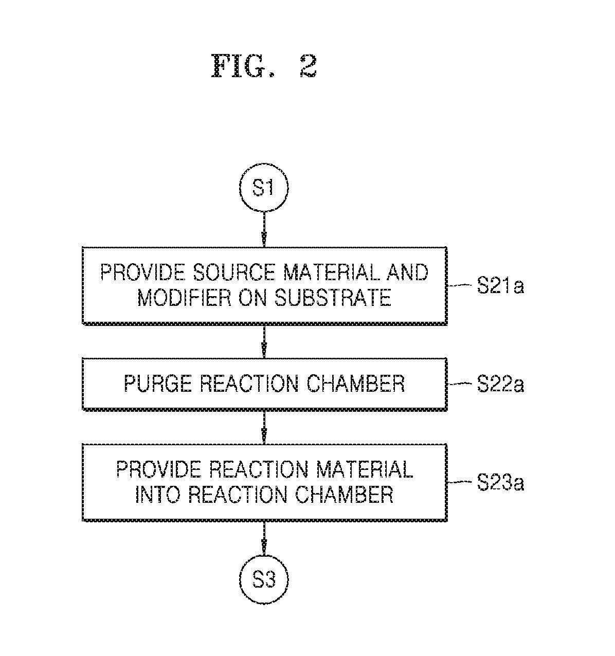
A method of forming a material layer includes providing a substrate into a reaction chamber, providing a source material onto a substrate, the source material being a precursor of a metal or semimetal having a ligand, providing an ether-based modifier on the substrate, purging an inside of the reaction chamber, and reacting a reaction material with the source material to form the material layer.

Description

CROSS-REFERENCE TO RELATED APPLICATION[0001]This application is a continuation-in-part under 35 U.S.C. §120 of U.S. application Ser. No. 15 / 227,089, filed Aug. 3, 2016, which claims the benefit of priority under 35 U.S.C. §119 from Korean Patent Application No. 10-2015-0110234, filed on Aug. 4, 2015, in the Korean Intellectual Property Office, the disclosure of each of which is incorporated herein in its entirety by reference.BACKGROUNDField[0002]Example embodiments of the inventive concepts relate to a semiconductor manufacturing apparatus, and more particularly, to a semiconductor manufacturing apparatus, by which a material layer having good step coverage may be stably manufactured despite variations in other process parameters.Related Art[0003]As semiconductor devices have been increasingly downscaled, it has become more difficult to conformally form thin layers. In particular, with the downscaling of semiconductor devices, aspect ratios of structures in semiconductor devices ma...

Claims


Application Information

Patent Timeline
IPC IPC(8): C23C16/455H01L21/02H01L21/28
CPCC23C16/45544C23C16/45525H01L21/28194H01L21/0228C23C16/45557C23C16/045C23C16/405C23C16/45534C23C16/45542C23C16/45561H01L21/02181H01L21/02186H01L21/02189H01L21/28088H01L28/90H01L29/7853H01L21/823431H10B43/27
Inventor MOON, SUN-MINKIM, YOUN-SOOLIM, HAN-JINLEE, YONG-JAEOH, SE-HOONKIM, HYUN-JUNLEE, JIN-SUN
Owner SAMSUNG ELECTRONICS CO LTD
Learn More