Method of fabricating acoustic wave device and acoustic wave device

a technology of acoustic wave and acoustic wave, which is applied in the direction of fluid pressure measurement, fluid pressure measurement by electric/magnetic elements, instruments, etc., can solve the problems of reducing the yield ratio, increasing the manufacturing cost, and difficult to process a plurality of wafers at the same tim

Active Publication Date: 2017-12-28
TAIYO YUDEN KK
View PDF3 Cites 57 Cited by
  • Summary
  • Abstract
  • Description
  • Claims
  • Application Information

AI Technical Summary

Benefits of technology

[0005]According to a first aspect of the present invention, there is provided a method of fabricating an acoustic wave device, the method including: forming on a piezoelectric substrate a comb-shaped electrode and a wiring layer coupled to the comb-shaped electrode; forming on the piezoelectric substrate a first dielectric film having a film thickness greater than those of the comb-shaped electrode and the wiring layer and covering the comb-shaped electrode and the wiring layer, the first dielectric film being made of silicon ox

Problems solved by technology

When the dielectric film is removed by dry etching, the manufacturing cost increases because the etching time of the dielectric film is long due to its relatively thick film thickness and it is difficult to process a pl

Method used


Image

  • Method of fabricating acoustic wave device and acoustic wave device
  • Method of fabricating acoustic wave device and acoustic wave device
  • Method of fabricating acoustic wave device and acoustic wave device

Examples


first embodiment

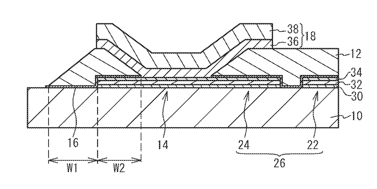
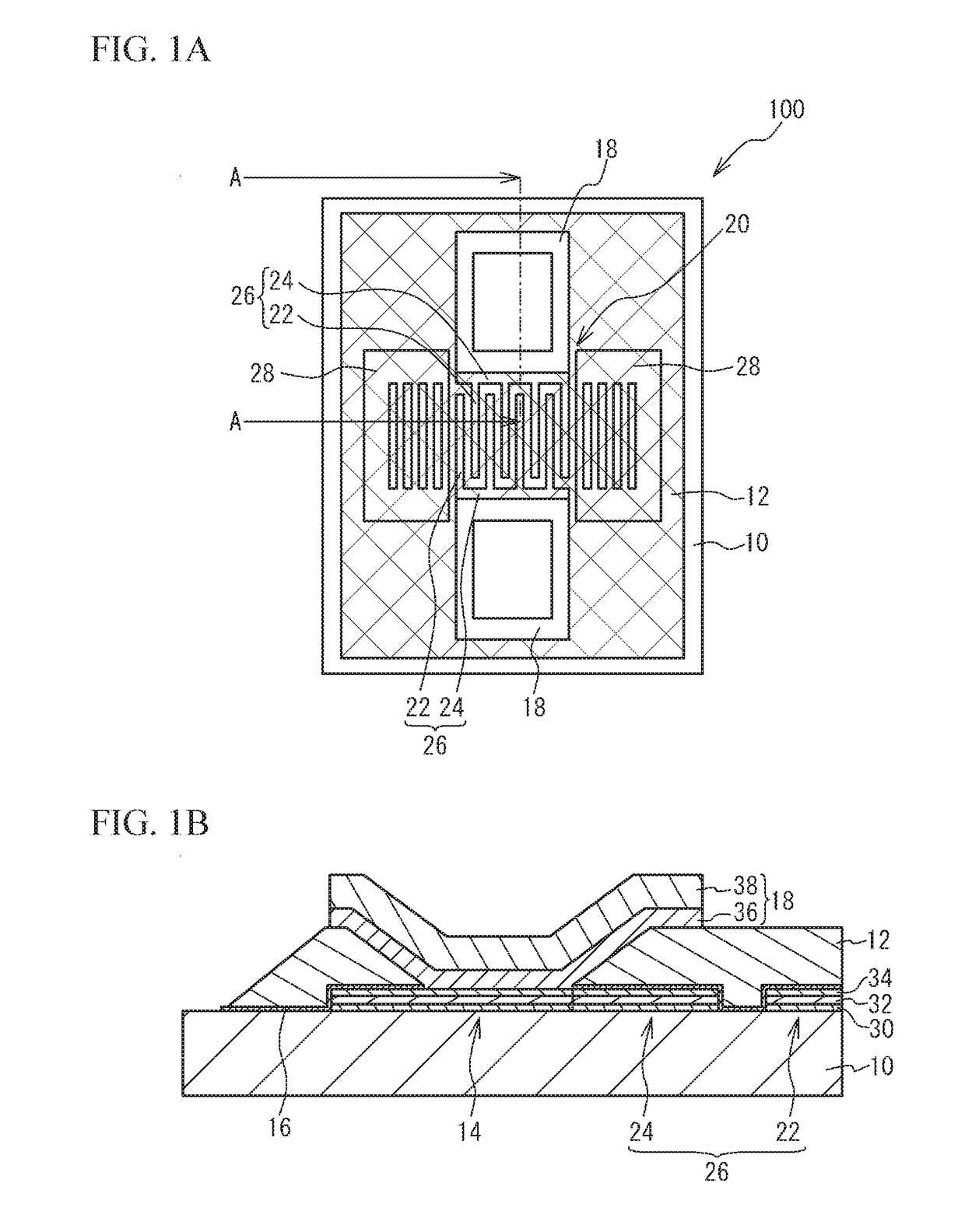
[0025]FIG. 1A is a plan view of an acoustic wave resonator in accordance with a first embodiment, and FIG. 1B is a cross-sectional view taken along line A-A in FIG. 1A. As illustrated in FIG. 1A and FIG. 1B, an acoustic wave resonator 100 of the first embodiment includes: an IDT 20 including a pair of comb-shaped electrodes 26; and reflectors 28 located at both sides of the IDT 20. The IDT 20 and the reflectors 28 are formed on a piezoelectric substrate 10. The piezoelectric substrate 10 can be, for example, a rotated Y-cut X-propagation lithium niobate (LN) substrate or a rotated Y-cut X-propagation lithium tantalate (LT) substrate. The cut angle can be appropriately configured depending on desired characteristics. For example, a 128° rotated Y-cut X-propagation LN substrate or a 42° rotated Y-cut X-propagation LT substrate can be employed.

[0026]The comb-shaped electrode 26 includes a plurality of electrode fingers 22 and a bus bar 24 to which the electrode fingers 22 are coupled. ...

second embodiment

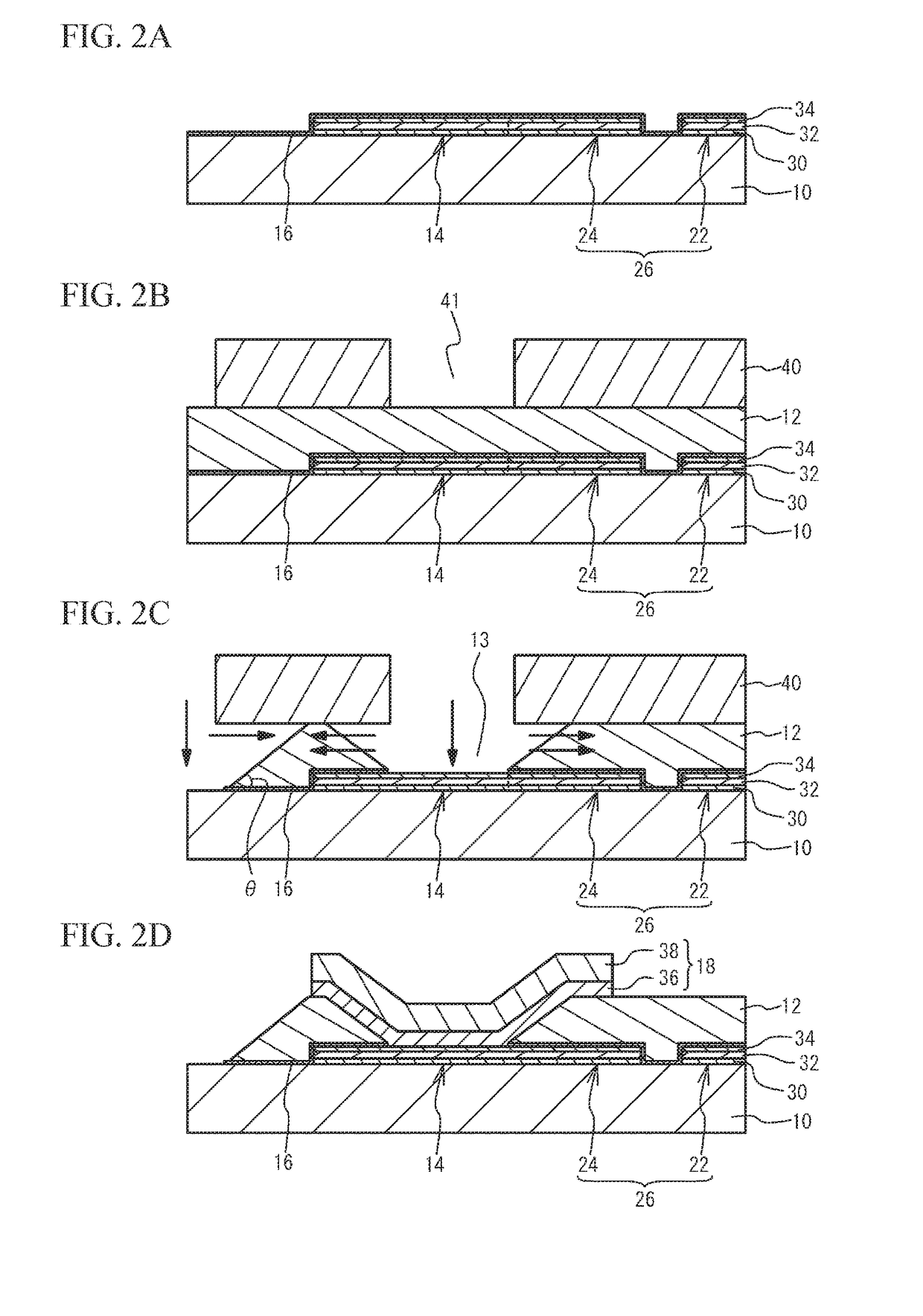
[0051]A description will be given of a problem that may arise in the acoustic wave resonator of the first embodiment. FIG. 6A and FIG. 6B are cross-sectional views for describing a problem that may arise in the acoustic wave resonator of the first embodiment. As illustrated in FIG. 6A, in the step of removing the dielectric film 12 by wet etching using the resist film 40 as a mask, since the dielectric film 12 exhibits hydrophobicity and the resist film 40 exhibits hydrophilicity, the adhesiveness between the dielectric film 12 and the resist film 40 is poor. Thus, an etching liquid may penetrate deeply into the boundary face between the dielectric film 12 and the resist film 40.

[0052]As illustrated in FIG. 6B, when the etching liquid penetrates deeply into the boundary face between the dielectric film 12 and the resist film 40, the dielectric film 12 above the comb-shaped electrodes 26 may be etched and removed. In addition, the further progression of the etching may erode the expo...

third embodiment

[0076]FIG. 12A is a plan view of a ladder-type filter in accordance with a third embodiment, and FIG. 12B is a plan view of a ladder-type filter in accordance with a first variation of the third embodiment. As illustrated in FIG. 12A, in a ladder-type filter 300 of the third embodiment, the dielectric film 50 above the edge portions of the electrodes constituting the series resonators S1 through S4 and the parallel resonators P1 through P3 and above the edge portions of the wiring layers 14 forms a thick film portion 52 that is thicker than the remaining portion. That is, the thick film portion 52 of the dielectric film 50 is located around the region where the dielectric film 12 is removed. The thick film portion 52 extends along the end faces of the wiring layers 14 so as to rim the wiring layers 14. Other structures are the same as those of the ladder-type filter 220 in FIG. 11A, and the description thereof is thus omitted. As illustrated in FIG. 12B, in a ladder-type filter 310 ...


PUM

PropertyMeasurementUnit
Thicknessaaaaaaaaaa

Abstract

An acoustic wave device fabrication method includes: forming on a piezoelectric substrate a comb-shaped electrode and a wiring layer coupled to the comb-shaped electrode; forming on the piezoelectric substrate a first dielectric film having a film thickness greater than those of the comb-shaped electrode and the wiring layer, covering the comb-shaped electrode and the wiring layer, and being made of silicon oxide doped with an element or undoped silicon oxide; forming on the first dielectric film a second dielectric film having an aperture above the wiring layer; removing the first dielectric film exposed by the aperture of the second dielectric film by wet etching using an etching liquid causing an etching rate of the second dielectric film to be less than that of the first dielectric film so that the first dielectric film is left so as to cover an end face of the wiring layer and the comb-shaped electrode.

Description

CROSS-REFERENCE TO RELATED APPLICATION[0001]This application is based upon and claims the benefit of priority of the prior Japanese Patent Application No. 2016-127527, filed on Jun. 28, 2016, the entire contents of which are incorporated herein by reference.FIELD[0002]A certain aspect of the present invention relates to a method of fabricating an acoustic wave device and an acoustic wave device.BACKGROUND[0003]It has been known that the temperature characteristics and electric characteristics of an acoustic wave device are improved by providing a predetermined shaped protective film covering a comb-shaped electrode located on a piezoelectric substrate as disclosed in, for example, Japanese Patent Application Publication No. 2009-201168. There has been also known an acoustic wave device in which a frequency adjusting film is located on a protective film covering a comb-shaped electrode as disclosed in, for example, Japanese Patent Application Publication No. 2013-145930.[0004]When a ...

Claims


Application Information

Patent Timeline
IPC IPC(8): G01L9/00H01L41/08G01L1/16H03H3/08H03H9/145H03H9/02
CPCG01L9/0025H03H3/08G01L1/165H01L41/08H03H9/02543H03H9/02842H03H9/145H03H9/02834Y10T29/49005Y10T29/42H03H3/02H03H3/0072H03H2003/023H03H2003/027H03H2003/025H10B12/033H10N30/00H10N30/06
Inventor NAKAMURA, KENTAROMATSUKURA, FUMIYATAKAHASHI, NAOKIMATSUDA, TAKASHIMIYASHITA, TSUTOMU
Owner TAIYO YUDEN KK
Why Eureka
Try Eureka