Diamond like carbon layer formed by an electron beam plasma process

a plasma process and electron beam technology, applied in diamond, chemical vapor deposition coating, coatings, etc., can solve the problems of insufficient masking, insufficient pattern transfer, and inability to accurately transfer the pattern for the manufacture of structures having small critical dimensions and high aspect ratios

Inactive Publication Date: 2017-12-28
APPLIED MATERIALS INC
View PDF4 Cites 24 Cited by
  • Summary
  • Abstract
  • Description
  • Claims
  • Application Information

AI Technical Summary

Benefits of technology

[0008]Methods for forming a diamond like carbon layer with desired film density, mechanical strength as well as optical film properties are provided. In one embodiment, a method of forming a diamond like carbon la...

Problems solved by technology

Integrated circuits have evolved into complex devices that can include millions of transistors, capacitors and resistors on a single chip.
As the geometry limits of the structures used to form semiconductor devices are pushed against technology limits, the need for accurate pattern transfer for the manufacture of structures having small critical dimensions and high aspect ratios has become increasingly difficult.
Such thin resist layers (e.g., less than about 2000 Å) can be insufficient to mask underlying material layers during the pattern transfer step due to attack by the chemical etchant.
After a long period of exposure to the aggressive etchants, the hardmask layer without sufficient etching resistance may be changed in film properties, resulting in inaccurate pattern transfer and loss of dimensional control.
Furthermore, the similarity of the materials selected for the...

Method used


Image

  • Diamond like carbon layer formed by an electron beam plasma process
  • Diamond like carbon layer formed by an electron beam plasma process
  • Diamond like carbon layer formed by an electron beam plasma process

Examples


Embodiment Construction

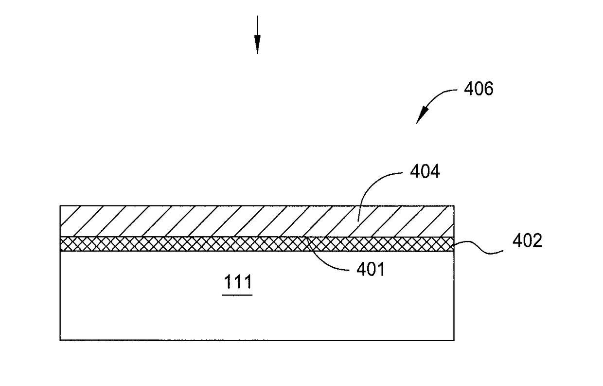
[0018]Embodiments of the present disclosure provide methods for forming a diamond like carbon layer with desired film properties, such as film transparency, mechanical strength, film hardness and low stress. In one embodiment, the diamond like carbon layer is suitable for use as a hardmask layer. The diamond like carbon layer with desired film properties may be obtained by an electron beam plasma deposition process. The electron beam plasma provides secondary electron beam required for depositing the carbon layer to form the carbon-like film structure with relatively strong bonding structure and mechanical strength. The diamond like carbon layer formed by the electron beam plasma maintains low stress level while having film density within a desired range. The diamond like carbon layer has optical film properties, such as a desired range of refraction index (n) and absorption coefficient (k), that are advantageous for photolithographic patterning processes.

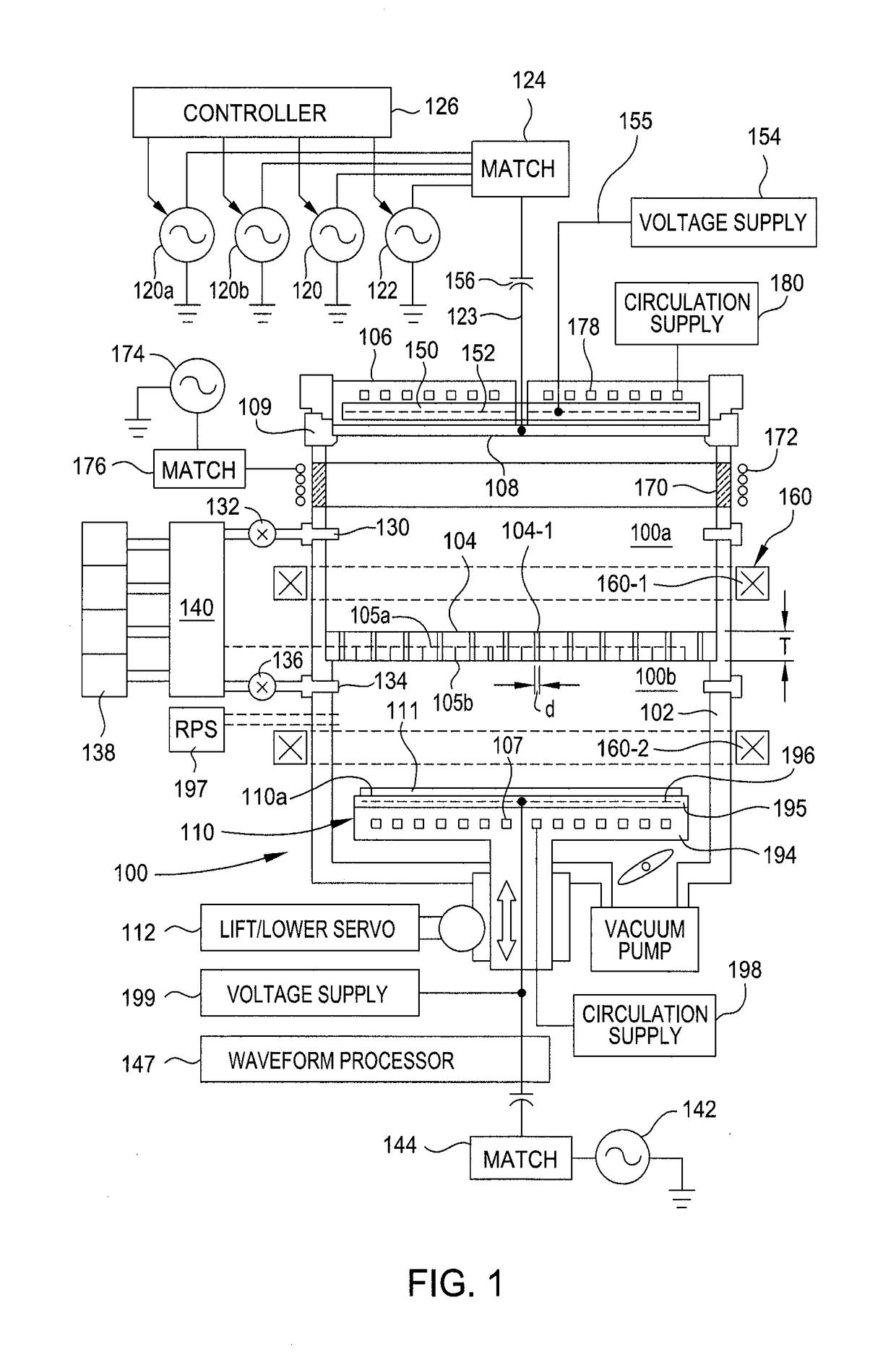
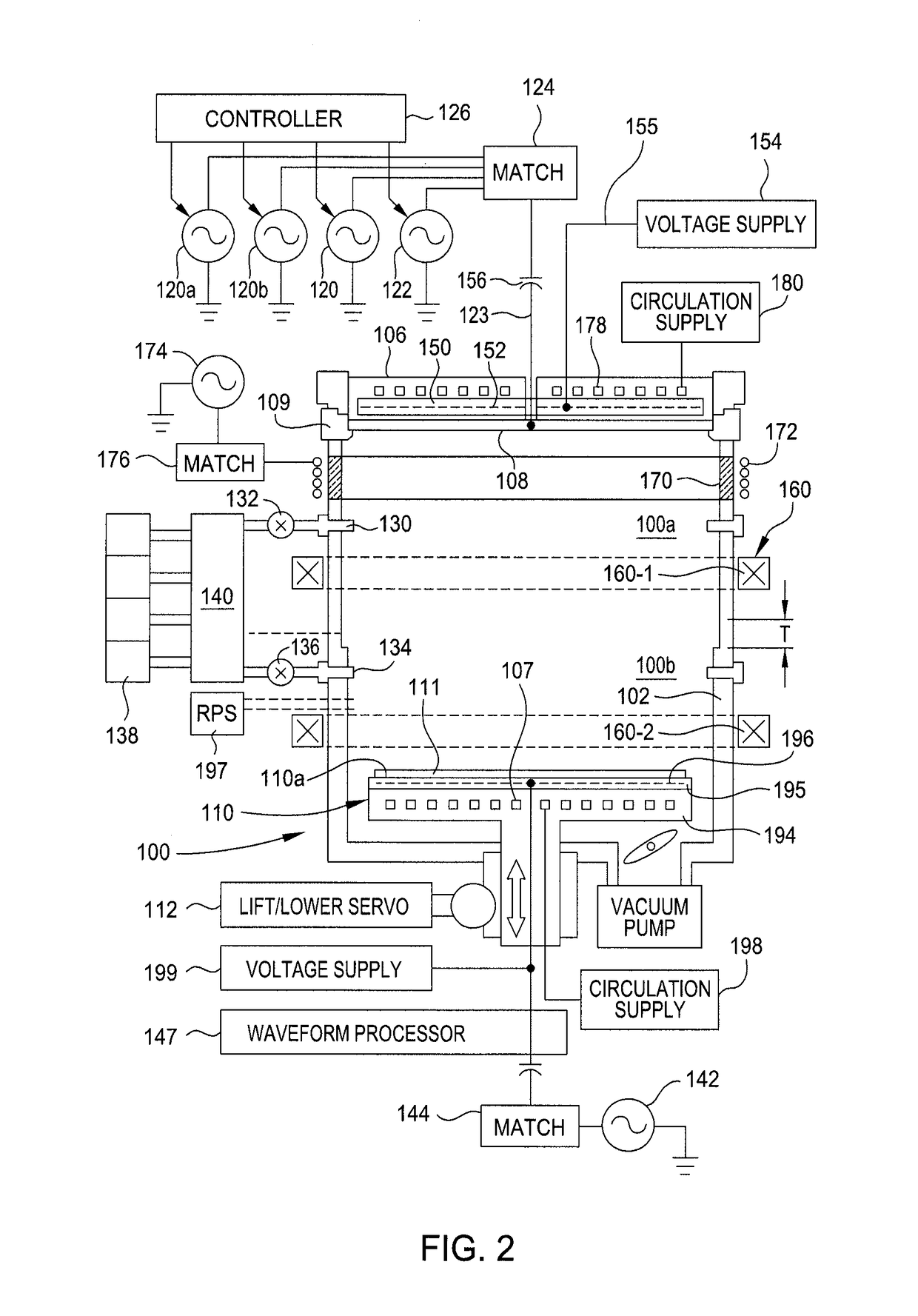
[0019]FIG. 1 depicts an ele...


PUM

PropertyMeasurementUnit
Temperatureaaaaaaaaaa
Densityaaaaaaaaaa
Energyaaaaaaaaaa

Abstract

Methods for forming a diamond like carbon layer with desired film density, mechanical strength and optical film properties are provided. In one embodiment, a method of forming a diamond like carbon layer includes generating an electron beam plasma above a surface of a substrate disposed in a processing chamber, and forming a diamond like carbon layer on the surface of the substrate. The diamond like carbon layer is formed by an electron beam plasma process, wherein the diamond like carbon layer serves as a hardmask layer in an etching process in semiconductor applications. The diamond like carbon layer may be formed by bombarding a carbon containing electrode disposed in a processing chamber to generate a secondary electron beam in a gas mixture containing carbon to a surface of a substrate disposed in the processing chamber, and forming a diamond like carbon layer on the surface of the substrate from elements of the gas mixture.

Description

BACKGROUNDField of the Disclosure[0001]The present disclosure relates to the fabrication of integrated circuits and to a process for forming a diamond like carbon layer with high etching selectivity, high film density and good mechanical strength on a substrate. More specifically, the disclosure relates to a process for manufacturing a diamond like carbon layer using electron beam plasma process to form the diamond like carbon layer with high etching selectivity, good mechanical strength, low stress and desired film transparency on a substrate for semiconductor applications.Description of the Background Art[0002]Integrated circuits have evolved into complex devices that can include millions of transistors, capacitors and resistors on a single chip. The evolution of chip designs continually requires faster circuitry and greater circuit density. The demands for faster circuits with greater circuit densities impose corresponding demands on the materials used to fabricate such integrate...

Claims


Application Information

Patent Timeline
IPC IPC(8): H01L21/033C23C16/505C23C16/509H01J37/32C23C16/26H01L21/308H01L21/02H01L21/3213C23C16/56H01L21/762
CPCH01L21/0332H01L21/76224C23C16/56H01J37/3255H01J37/32357C23C16/509C23C16/505C01B31/06H01L21/0337H01L21/3081H01L21/3086H01L21/32139H01L21/02115H01L21/02274H01J37/3266H01J37/32623H01J2237/327H01J2237/3321C23C16/26C01B32/25H01J37/3233H01J37/32422H01L21/0234H01J37/32174H01L21/3065
Inventor YANG, YANGCHEN, LUCYZHOU, JIERAMASWAMY, KARTIKCOLLINS, KENNETH S.NEMANI, SRINIVAS D.YING, CHENTSAULIU, JINGJINGLANE, STEVENMONROY, GONZALOCARDUCCI, JAMES D.
Owner APPLIED MATERIALS INC
Why Eureka
Try Eureka