Micro-selective sintering laser systems and methods thereof

a laser system and laser technology, applied in the direction of soldering apparatus, semiconductor/solid-state device details, manufacturing tools, etc., can solve the problems of low through-put that is not yet viable for commercial use, formation of defects in the final produced part, and too coarse resolution of feature size to precisely control the microstructure of parts desired to be produced

Active Publication Date: 2018-03-08
BOARD OF RGT THE UNIV OF TEXAS SYST
View PDF6 Cites 23 Cited by
  • Summary
  • Abstract
  • Description
  • Claims
  • Application Information

AI Technical Summary

Benefits of technology

[0022]In some embodiments, the exemplified systems and methods provides ability to achieve + / −5 μm flip chip alignment accuracy, e.g., for high-quality flexible electronic packages.

Problems solved by technology

In many applications, e.g., microelectronic packaging, among others, these feature-size resolutions are too coarse to precisely control microstructures of parts desired to be produced.
Existing research-based systems for metal additive manufacturing may fabricate finer resolutions features, but have low through-put that are not yet viable for commercial use.
Because of their size, agglomeration of nanoparticles (e.g., nanoparticle powder) can form, which can lead to the formation of defects in the final produced part.
In addition to agglomeration, at the sub-micron (μm) level, the interaction between nanoparticles (e.g., nanoparticle powder) under high power laser heating raises additional near-field thermal issues such as thermal diffusivity, effective absorptivity, and extinction coefficients as compared to larger scales processes.
The integration of such complex devices onto flexible substrates of requires high input / output (I / O) pin counts of these devices that can carry the high quality analog signals required by many of these components.

Method used


Image

  • Micro-selective sintering laser systems and methods thereof
  • Micro-selective sintering laser systems and methods thereof
  • Micro-selective sintering laser systems and methods thereof

Examples


Embodiment Construction

[0111]The nanoparticle powder and nanoparticle ink described herein may be understood more readily by reference to the following detailed description of specific aspects of the disclosed subject matter and the Examples included therein.

[0112]Before the present nanoparticle powder and nanoparticle ink are disclosed and described, it is to be understood that the aspects described below are not limited to specific synthetic methods or specific reagents, as such may, of course, vary. It is also to be understood that the terminology used herein is for the purpose of describing particular aspects only and is not intended to be limiting.

[0113]Also, throughout this specification, various publications are referenced. The disclosures of these publications in their entireties are hereby incorporated by reference into this application in order to more fully describe the state of the art to which the disclosed matter pertains. The references disclosed are also individually and specifically incor...


PUM

PropertyMeasurementUnit
spot sizeaaaaaaaaaa
feature-size resolutionsaaaaaaaaaa
sizesaaaaaaaaaa

Abstract

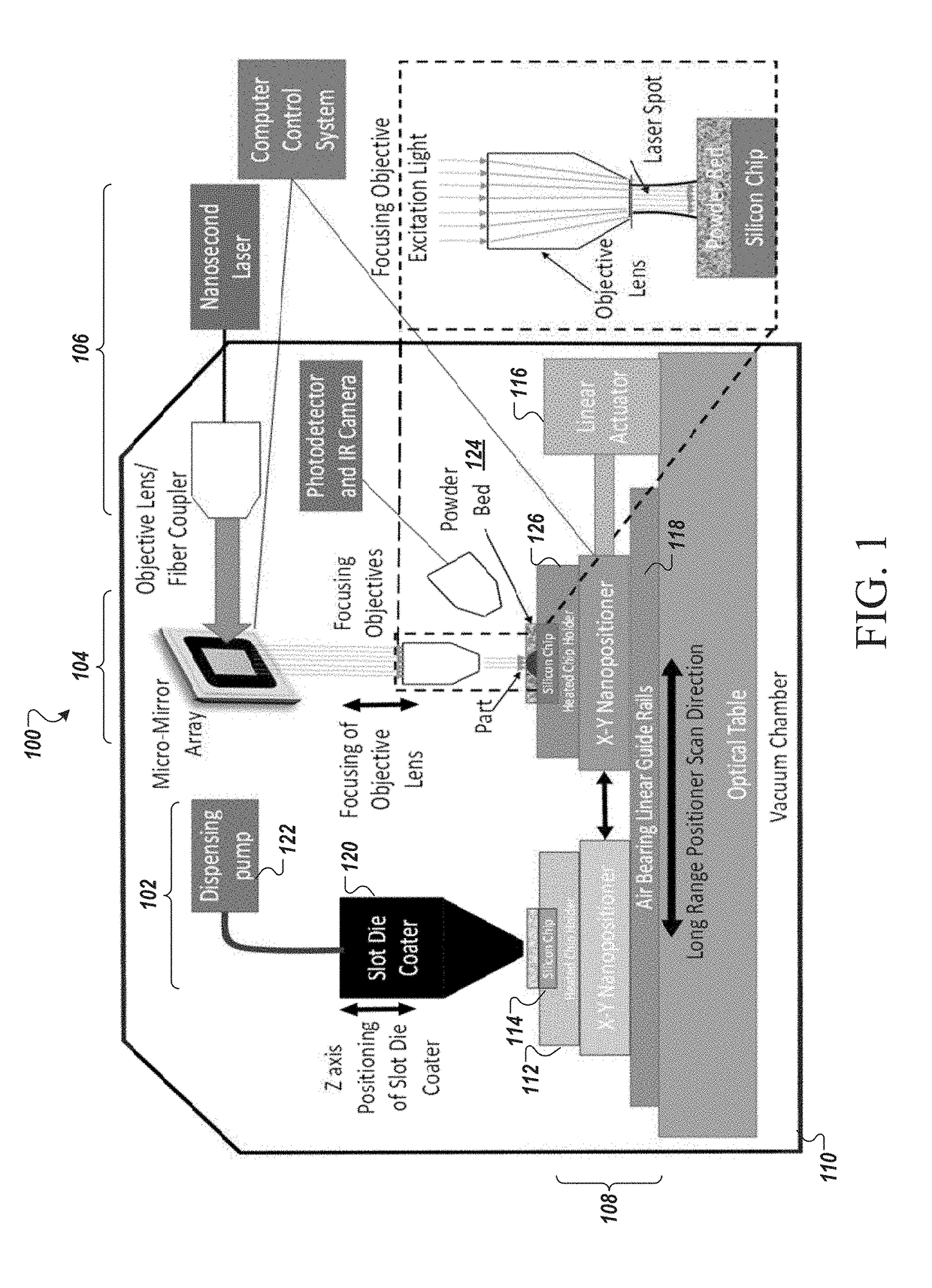
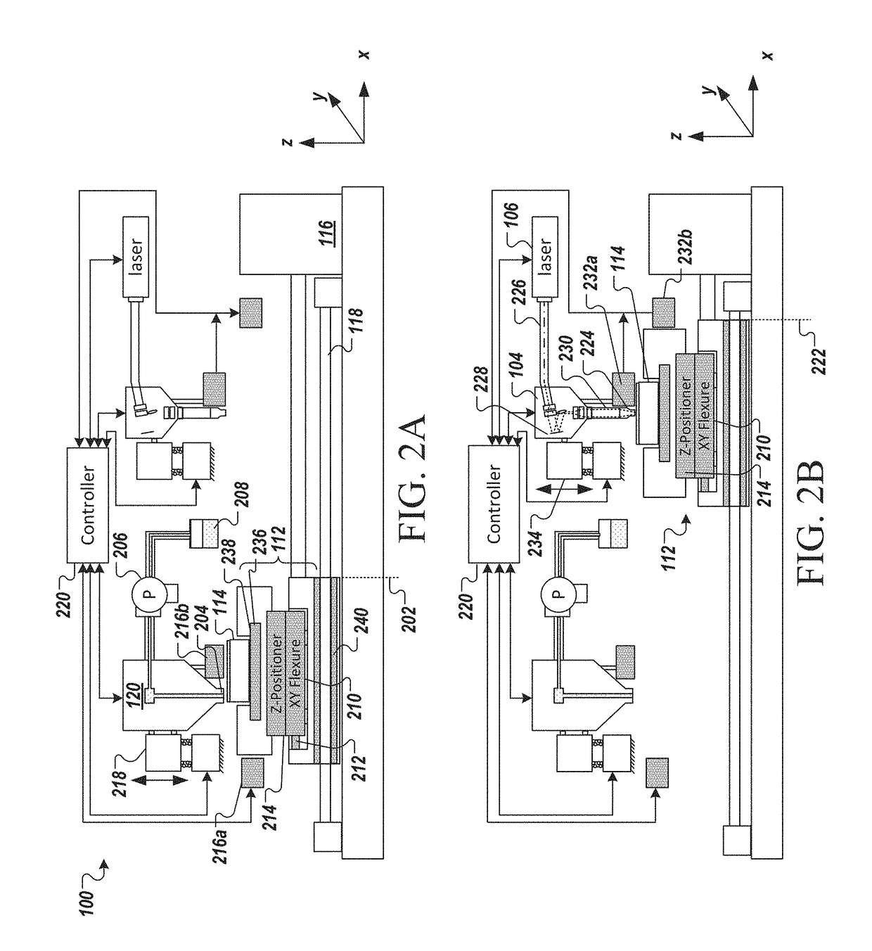
A microscale selective laser sintering (μ-SLS) that improves the minimum feature-size resolution of metal additively manufactured parts by up to two orders of magnitude, while still maintaining the throughput of traditional additive manufacturing processes. The microscale selective laser sintering includes, in some embodiments, ultra-fast lasers, a micro-mirror based optical system, nanoscale powders, and a precision spreader mechanism. The micro-SLS system is capable of achieving build rates of at least 1 cm3/hr while achieving a feature-size resolution of approximately 1 μm. In some embodiments, the exemplified systems and methods facilitate a direct write, microscale selective laser sintering μ-SLS system that is configured to write 3D metal structures having features sizes down to approximately 1 μm scale on rigid or flexible substrates. The exemplified systems and methods may operate on a variety of material including, for example, polymers, dielectrics, semiconductors, and metals.

Description

RELATED APPLICATIONS[0001]This application claims priority to, and the benefit of, U.S. Provisional Appl. No. 62 / 316,644, filed Apr. 1, 2016, title “Micro-Selective Sintering Laser System and Method Thereof”; U.S. Provisional Appl. No. 62 / 316,666, filed Apr. 1, 2016, title “Modeling of Nanoparticle Agglomeration and Powder Bed Formation in Microscale Laster Sintering Systems”; and U.S. Provisional Appl. No. 62 / 454,456, filed Feb. 3, 2017, title “Micro-selective Sintering Laser on Flexible Substrates and With Multi-Material Capabilities,” each of which is incorporated by reference herein in its entirety.BACKGROUND[0002]Micro- and nano-scale additive manufacturing methods in metals, plastics, and ceramics have many applications in the aerospace, medical device, and electronics industries. For example, the fabrication of additively-manufactured parts with micron-scale resolutions makes possible the production of cellular materials with controlled microstructures. Such materials can exh...

Claims


Application Information

Patent Timeline
Patent Type & Authority Applications(United States)
IPC IPC(8): B22F7/02H01L23/00B33Y30/00B33Y50/02B33Y80/00B22F3/105B23K1/00H01L21/48H01L21/56H01L21/67H01L23/31H01L23/498B33Y10/00B22F1/00B23K101/36H01L21/683H01L23/544
CPCB22F7/02H01L2224/83939B33Y30/00B33Y50/02B33Y80/00B22F3/1055B23K1/0008H01L21/67115H01L21/4857H01L23/4985H01L21/4853H01L21/565H01L24/83H01L21/563H01L24/92H01L24/81H01L23/3135B22F2003/1056B23K2201/36B22F1/0044B22F2003/1059H01L21/6838H01L21/67144H01L23/544H01L2224/83132H01L2223/54426H01L2224/83007H01L2224/75101H01L2224/75901H01L2224/7501H01L2224/9211H01L2224/81132H01L2224/81007H01L2224/81815H01L2224/81224H01L2224/81192H01L2224/83054H01L2224/83224H01L2224/81054H01L24/75H01L2224/75261H01L2224/81908H01L2224/83908B33Y10/00B33Y70/00B22F2999/00B23K2101/36G06F30/23Y02P10/25B22F12/17B22F12/49B22F12/44B22F10/28B22F10/36B22F12/53B22F12/22B22F10/68B22F10/73B22F12/90B22F12/45B22F1/054B22F10/20B22F1/0545B22F1/07
Inventor CULLINAN, MICHAEL A.ROY, NILABH KUMARYUKSEL, ANILFOONG, CHEE SENG
Owner BOARD OF RGT THE UNIV OF TEXAS SYST
Why Eureka
Try Eureka