Auxiliary exposure apparatus and exposure amount distribution acquisition method

a technology of exposure amount and exposure amount, which is applied in the direction of photomechanical equipment, semiconductor/solid-state device testing/measurement, instruments, etc., can solve the problems of inability to obtain desired exposure amount, and difficult to achieve uniform line width of resist pattern obtained on wafer after developing treatment. achieve the effect of improving the in-plane uniform line width of resist pattern

Active Publication Date: 2018-04-05
TOKYO ELECTRON LTD
View PDF4 Cites 2 Cited by
  • Summary
  • Abstract
  • Description
  • Claims
  • Application Information

AI Technical Summary

Benefits of technology

[0017]According to the present invention, it is possible to further reliably improve the in-plane uniformity of the line width of the resist pattern.

Problems solved by technology

Incidentally, with advancement of microfabrication of the pattern by the photolithography, making the line width of the resist pattern obtained on the wafer after the developing treatment uniform becomes more difficult, and the in-plane uniformity of the line width of the resist pattern is a major problem.
This method, however, performs exposure using the slit of N mm×25 mm, and therefore can change the exposure amount in a direction in which the slit is scanned, but cannot change the exposure amount in one exposure shot.
Further, the width of the slit in the scan direction is also as large as about several millimeters, and the adjustment of the exposure amount in the scan direction is not sufficient, thus leaving room for improvement in terms of in-plane uniformity of the line width of the resist pattern.
However, even if the output of the light source at the time of auxiliary exposure is adjusted as described above, the desired exposure amount cannot be obtained in each divided irradiation area on the wafer upper surface in some cases because the light path from the light source to each divided irradiation area is different.
Accordingly, the state of the light path from the light source to each irradiation area on the wafer upper surface changes between measurements due to change in apparatus environment or the like, and the desired illuminance to the command value of the light output, namely, exposure amount cannot be obtained any longer, possibly resulting in decreased in-plane uniformity of the line width of the resist pattern.

Method used


Image

  • Auxiliary exposure apparatus and exposure amount distribution acquisition method
  • Auxiliary exposure apparatus and exposure amount distribution acquisition method
  • Auxiliary exposure apparatus and exposure amount distribution acquisition method

Examples


first embodiment

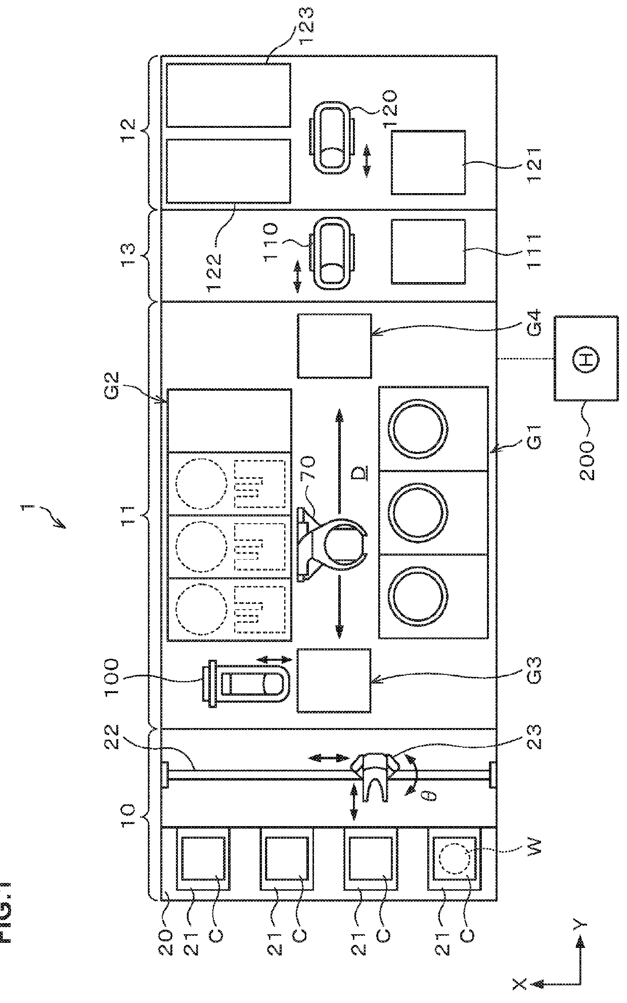
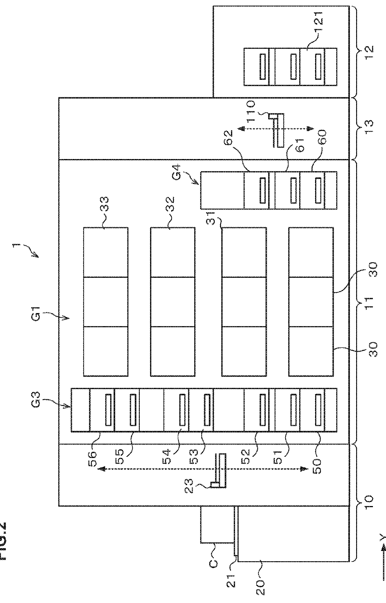
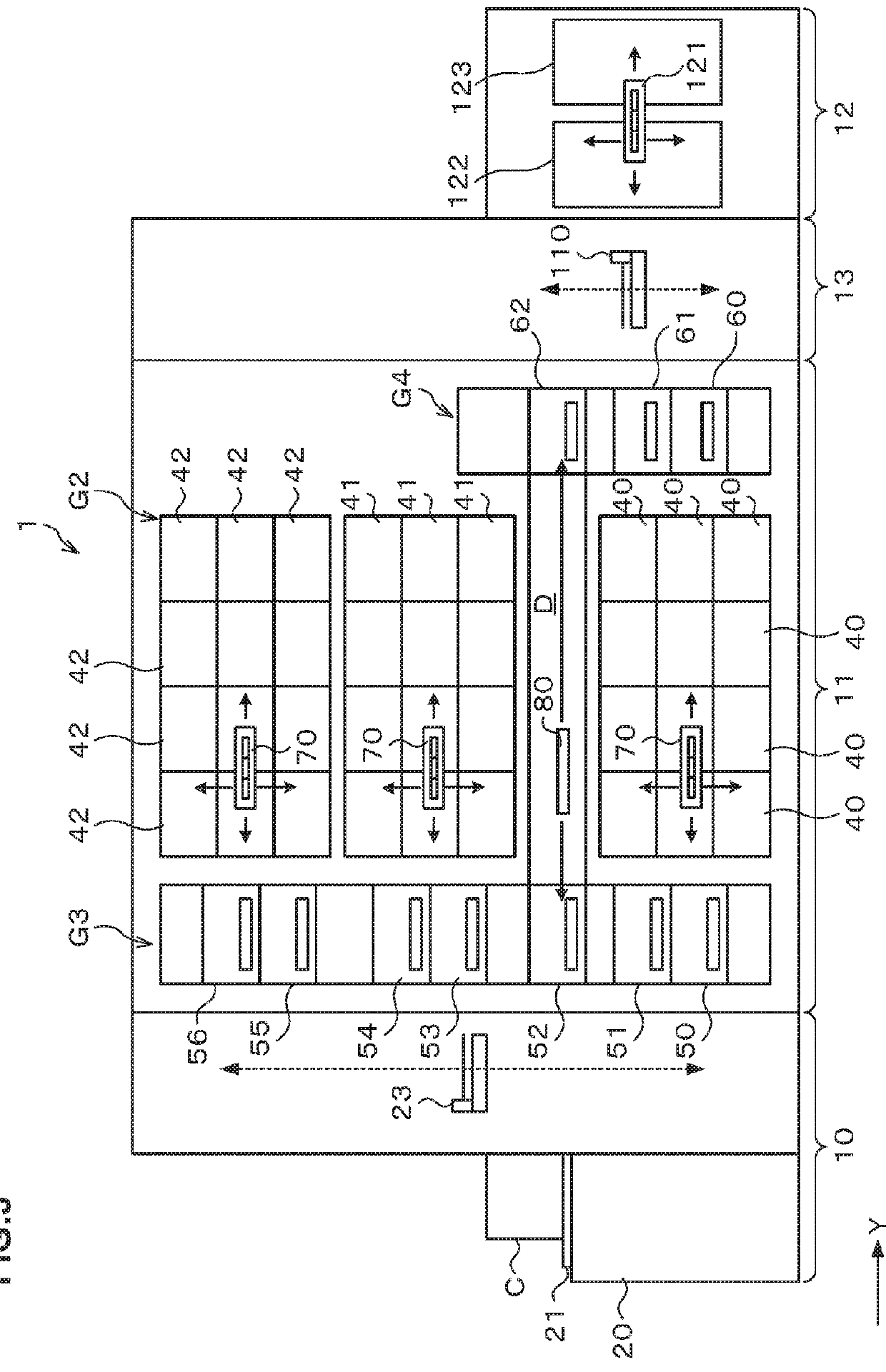
[0030]Hereinafter, embodiments of the present invention will be described. FIG. 1 is an explanatory view illustrating the outline of a configuration of a substrate processing system 1 equipped with an exposure station including an auxiliary exposure apparatus according to a first embodiment of the present invention. FIG. 2 and FIG. 3 are a front view and a rear view schematically illustrating the outline of an internal configuration of the substrate processing system 1, respectively. Note that in this specification and the drawings, components having substantially the same functional configurations are denoted by the same signs to omit duplicate description.

[0031]The substrate processing system 1 has, as illustrated in FIG. 1, a configuration in which a cassette station 10 into / out of which a cassette C housing a plurality of wafers W is carried, a treatment station 11 which includes a plurality of various treatment apparatuses performing predetermined treatments on the wafer W, and...

second embodiment

[0106]FIG. 10 is a view for explaining the outline of a configuration of an auxiliary exposure apparatus according to a second embodiment of the present invention.

[0107]The auxiliary exposure apparatus 123 in FIG. 10 has a multi-reflection preventing plate 150. The multi-reflection preventing plate 150 is a multi-reflection preventing plate that prevents the light applied to and irregularly reflected by the wafer W from being reflected again by the first total reflection mirror 141 and / or the second total reflection mirror 142 and returning to the wafer W.

[0108]FIG. 11 is a view for explaining the multi-reflection preventing plate 150 with only the multi-reflection preventing plate 150 illustrated in a cross section.

[0109]The multi-reflection preventing plate 150 has, as illustrated in FIG. 11, for example, a first slit 151 through which the light reflected by the polygon mirror 139 (see FIG. 5), reflected by the first total reflection mirror 141, and directed toward the wafer W pas...


PUM

PropertyMeasurementUnit
wavelengthaaaaaaaaaa
diameteraaaaaaaaaa
diameteraaaaaaaaaa

Abstract

An auxiliary exposure apparatus is for performing auxiliary exposure of applying light of a predetermined wavelength from a laser light source to a resist film on a wafer, separately from exposure processing of transferring a pattern of a mask to the resist film applied on the wafer, and includes: a first total reflection mirror configured to reflect the light from the laser light source toward the wafer; and an imaging device including a light receiving part configured to receive light after reflected by the wafer.

Description

CROSS REFERENCE TO RELATED APPLICATIONS[0001]This application is based upon and claims the benefit of priority of the prior Japanese Patent Application No. 2016-196342, filed in Japan on Oct. 4, 2016, the entire contents of which are incorporated herein by reference.BACKGROUND OF THE INVENTION1. Field of the Invention[0002]The present invention relates to an auxiliary exposure apparatus that performs auxiliary exposure of applying an ultraviolet ray separately from normal exposure processing of transferring a pattern of a mask to a resist film applied on a substrate, and an exposure amount distribution acquisition method of acquiring an exposure amount distribution in auxiliary exposure.2. Description of the Related Art[0003]In a photolithography process in a manufacturing process of a semiconductor device or the like, a resist coating treatment of applying a resist solution onto a substrate such as a semiconductor wafer (hereinafter, referred to as a wafer) to form a resist film, e...

Claims


Application Information

Patent Timeline
Patent Type & Authority Applications(United States)
IPC IPC(8): G03F7/20G03F7/16H01L21/67G03F7/40H01L21/027
CPCG03F7/70991G03F7/168H01L21/67253G03F7/40H01L21/027H01L21/67248H01L22/20G03F7/2022H01L21/67178H01L21/67225H01L21/0274G03F7/2004G03F7/70233G03F7/70516
Inventor KASHIWAGI, HIDEAKINIWA, TAKAFUMIKOGA, NORIHISA
Owner TOKYO ELECTRON LTD
Why Eureka
Try Eureka