Three-Dimensional Imaging For Semiconductor Wafer Inspection

a three-dimensional imaging and semiconductor technology, applied in the direction of image enhancement, semiconductor/solid-state device testing/measurement, instruments, etc., can solve the problems of difficult detection of defects buried in relatively thick layers, difficult to detect defects in the presence of buried defects, and difficult to achieve sem review. often unfavorable, improve the detection and classification of defects, and improve the effect of detection and classification

Active Publication Date: 2018-04-12
KLA CORP
View PDF4 Cites 30 Cited by
  • Summary
  • Abstract
  • Description
  • Claims
  • Application Information

AI Technical Summary

Benefits of technology

[0014]Methods and systems for improved detection and classification of defects of interest (DOI) on semiconductor wafers based on three-dimensional images are described herein. Three dimensional imaging of volumes of thick, layered structures enables accurate defect detection and estimation of defect location in three dimensions at high throughput. Traditionally, signals arising from acceptable wafer variation (e.g., nuisance and noise) often limit detection of DOIs. However, three-dimensional imaging captures signal propagation within the wafer, and thus is able to differentiate DOIs from nuisance and noise, even for relatively thick samples (e.g., 3D NAND wafers with a layered structure thicker than three micrometers). In some examples, optical inspection of thick samples based on three dimensional imaging differentiates defects of interest residing on one layer from nuisance and noise originating from other layers.
[0020]In a further aspect, the three dimensional image is filtered before defect analysis to improve SNR. In some examples, computing system analyzes the assembled three-dimensional image with a 3D digital filter, or other suitable numerical technique to detect unique three-dimensional structures arising from defects. This effectively increases the SNR of the defects and enables more effective separation of defects of interest from noise or nuisance effects.
[0021]In another further aspect, illumination apertures, collection apertures, or both, are tuned to minimize the response of the nominal structure and enhance the response of the defect signal.

Problems solved by technology

Such high aspect ratio structures create challenges for patterned wafer inspection.
These techniques are fast enough to catch defects-of-interest (DOI) for thin layers (e.g., less than one micrometer thick), but are less effective for the detection of defects buried in relatively thick layers.
SEM review is often unfeasible for buried defects.
However, important signal information resulting from the interaction of structures within the focal plane and structures above and below the focal plane is also lost.
This loss of signal information may inhibit the ability to measure defect depth accurately and eliminate unwanted optical signals with a strong signal-to-noise ratio (SNR).
However, the ability to measure weak defects is limited by splitting the optical intensity, thereby limiting sensitivity.
Additionally, the resulting images are complicated, and it is difficult to interpret the effect of the wafer structure on the incident and collected optical fields.
Thus, defects cannot be detected early in the production cycle, resulting in lost time and expense.
As a result, electronic tests are prohibitively expensive to perform on all lots during all steps in the production process, including research and development, production ramp, and high volume manufacture.
Unfortunately, for some layers in the 3D NAND process, electronic tests have been the only solution.
This approach requires alternate process flows at each layer, and the alternate processes may produce defects that interfere with DOI detection.
In addition, some DOI on some layers are not easily revealed by wafer de-processing.
EBI is limited in throughput and wafer coverage and may only be performed on some layers in the 3D NAND process.
Thus, EBI is limited in its effectiveness as a defect detection tool for three dimensional structures.
Traditionally, signals arising from acceptable wafer variation (e.g., nuisance and noise) often limit detection of DOIs.

Method used


Image

  • Three-Dimensional Imaging For Semiconductor Wafer Inspection
  • Three-Dimensional Imaging For Semiconductor Wafer Inspection
  • Three-Dimensional Imaging For Semiconductor Wafer Inspection

Examples


Embodiment Construction

[0042]Reference will now be made in detail to background examples and some embodiments of the invention, examples of which are illustrated in the accompanying drawings.

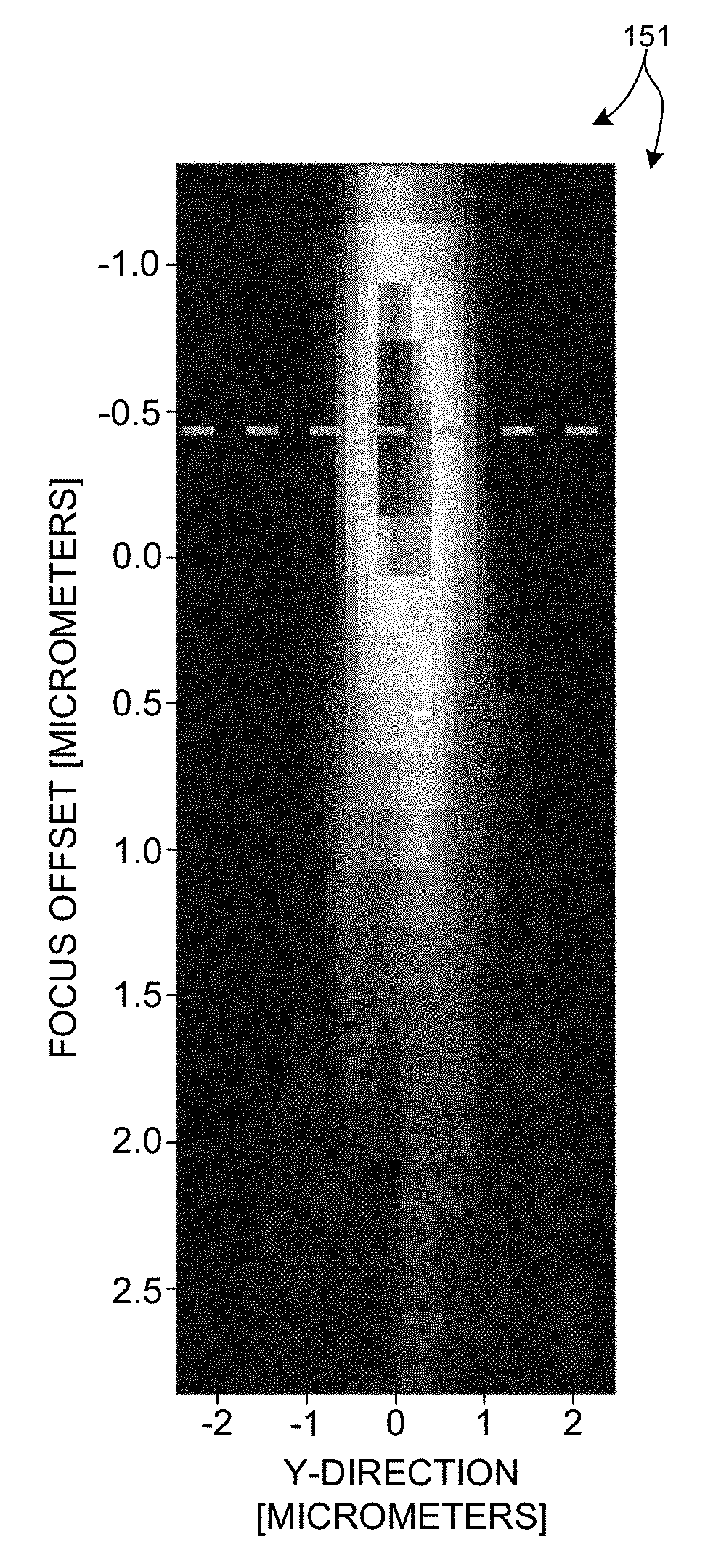
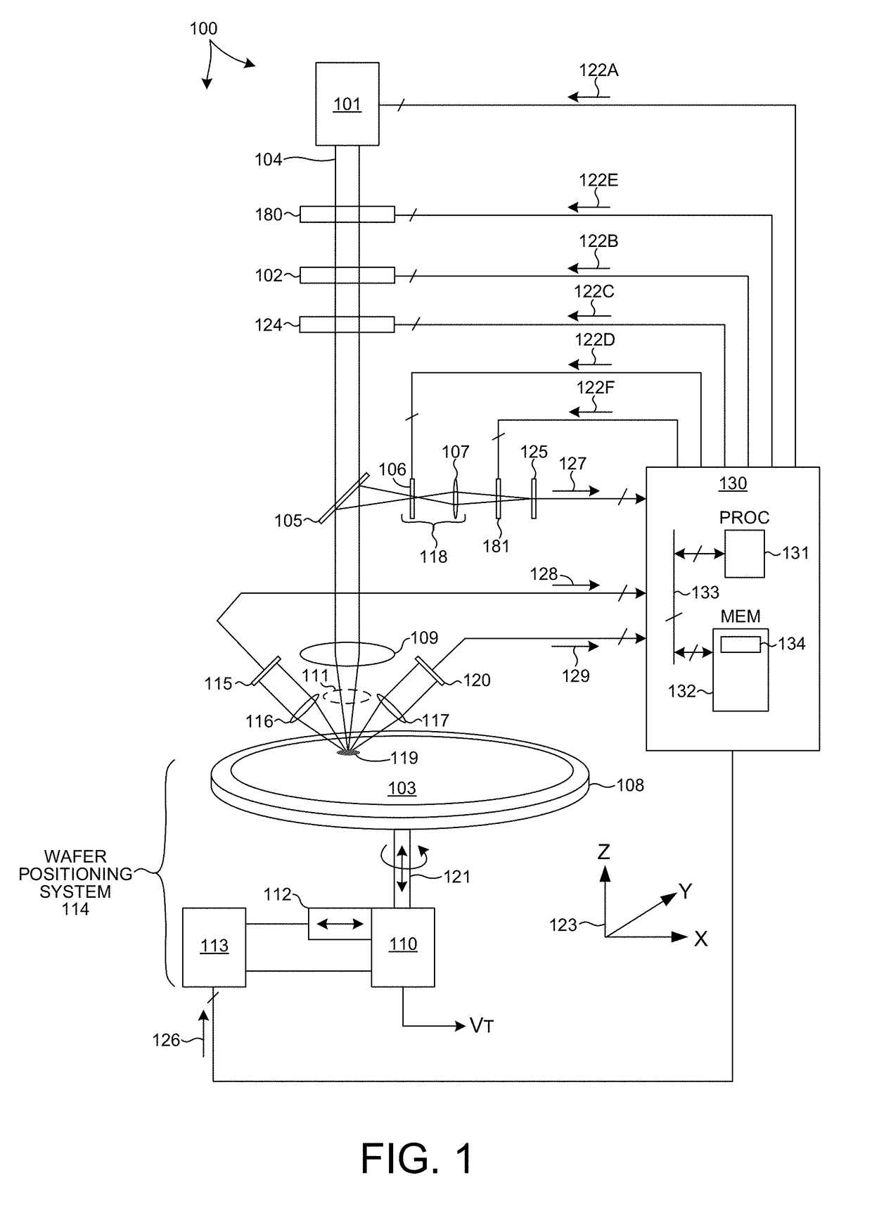
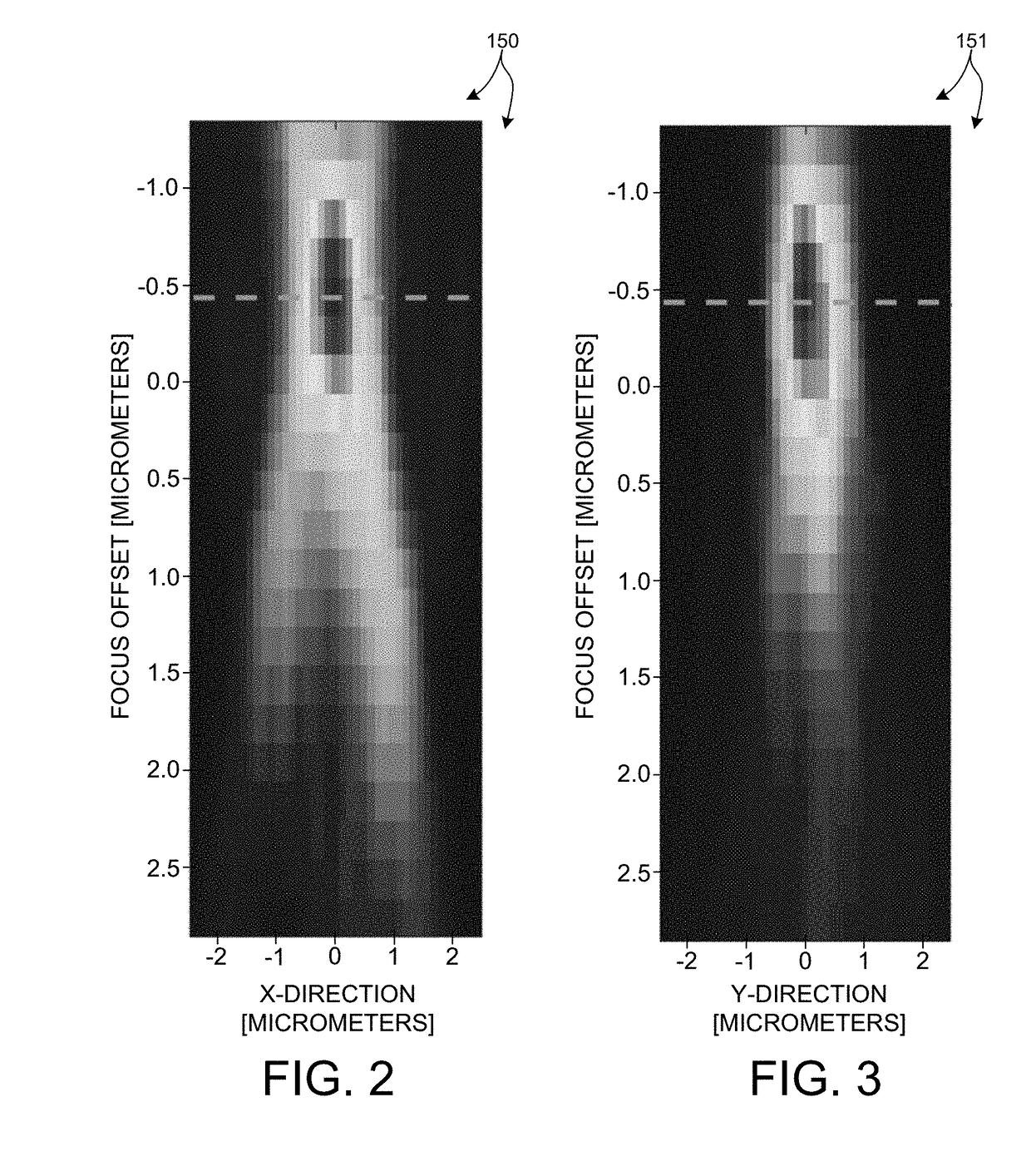
[0043]Methods and systems for improved detection and classification of defects of interest (DOI) on semiconductor wafers based on three-dimensional images are described herein. Three dimensional imaging of volumes of thick, layered structures enables accurate defect detection and estimation of defect location in three dimensions at high throughput. Traditionally, signals arising from acceptable wafer variation (e.g., nuisance and noise) often limit detection of DOIs. However, three-dimensional imaging captures signal propagation within the wafer, and thus is able to differentiate DOIs from nuisance and noise, even for relatively thick samples (e.g., 3D NAND wafers with a layered structure thicker than three micrometers). In some examples, optical inspection of thick samples based on three dimensional imaging different...


PUM

PropertyMeasurementUnit
wavelengthsaaaaaaaaaa
depthaaaaaaaaaa

Abstract

Methods and systems for improved detection and classification of defects of interest (DOI) on semiconductor wafers based on three-dimensional images are described herein. Three dimensional imaging of volumes of thick, layered structures enables accurate defect detection and estimation of defect location in three dimensions at high throughput. A series of images are acquired at a number of different wafer depths. A three dimensional image of a thick semiconductor structure is generated from the series of images. Defects are identified and classified based on an analysis of the three dimensional image of the thick semiconductor structure. In some examples, the three-dimensional image stack is visualized by contour plots or cross-sectional plots to identify a characteristic defect response. In some examples, the three-dimensional image is processed algorithmically to identify and classify defects. In another aspect, the location of a defect is estimated in three dimensions based on the three dimensional image.

Description

CROSS REFERENCE TO RELATED APPLICATION[0001]The present application for patent claims priority under 35 U.S.C. § 119 from U.S. provisional patent application Ser. No. 62 / 405,435, filed Oct. 7, 2016, the subject matter of which is incorporated herein by reference in its entirety.TECHNICAL FIELD[0002]The described embodiments relate to systems for specimen inspection, and more particularly to semiconductor wafer inspection modalities.BACKGROUND INFORMATION[0003]Semiconductor devices such as logic and memory devices are typically fabricated by a sequence of processing steps applied to a substrate or wafer. The various features and multiple structural levels of the semiconductor devices are formed by these processing steps. For example, lithography among others is one semiconductor fabrication process that involves generating a pattern on a semiconductor wafer. Additional examples of semiconductor fabrication processes include, but are not limited to, chemical-mechanical polishing, etch...

Claims


Application Information

Patent Timeline
Patent Type & Authority Applications(United States)
IPC IPC(8): H04N13/02G01N21/95G06V10/141H04N13/221
CPCH04N13/0253G01N21/9505H04N13/0271H04N13/0221G06T7/0008G06T2207/10028G06T2207/30148G06K9/6267G06T7/70G06K9/40G01N2021/8438G06T5/50G06T7/0004G06T2207/10148G06T2207/20221G01N21/956G01N2021/8861H04N13/254H04N13/271H04N13/221G06T2207/20084G06V10/141H01L22/12H01L22/24H01L22/30G06F18/24
Inventor KOLCHIN, PAVELDANEN, ROBERT M.MEASOR, PHILIP
Owner KLA CORP
Why Eureka
Try Eureka