Control circuit and control method for switch power supply, and switch power supply
- Summary
- Abstract
- Description
- Claims
- Application Information
AI Technical Summary
Benefits of technology
Problems solved by technology
Method used
Image
Examples
first embodiment
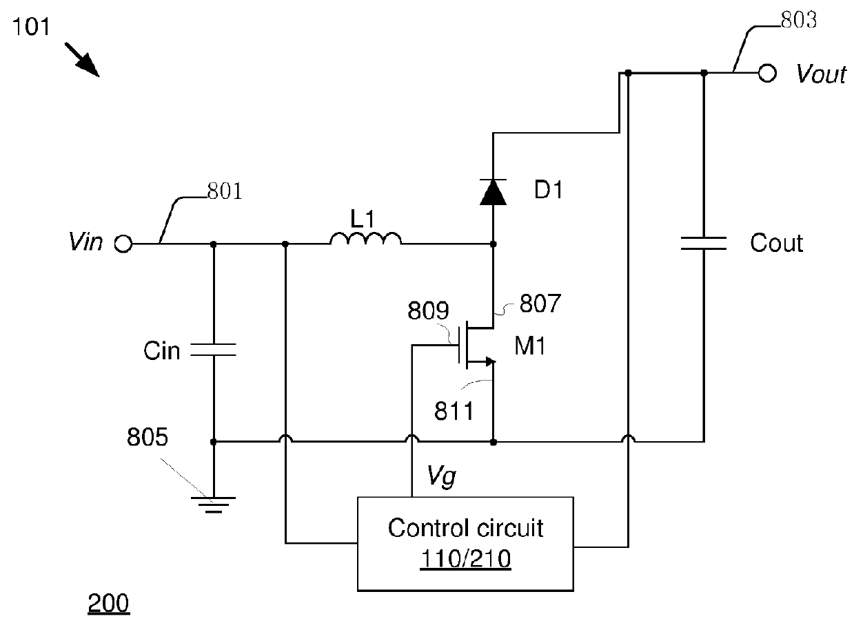
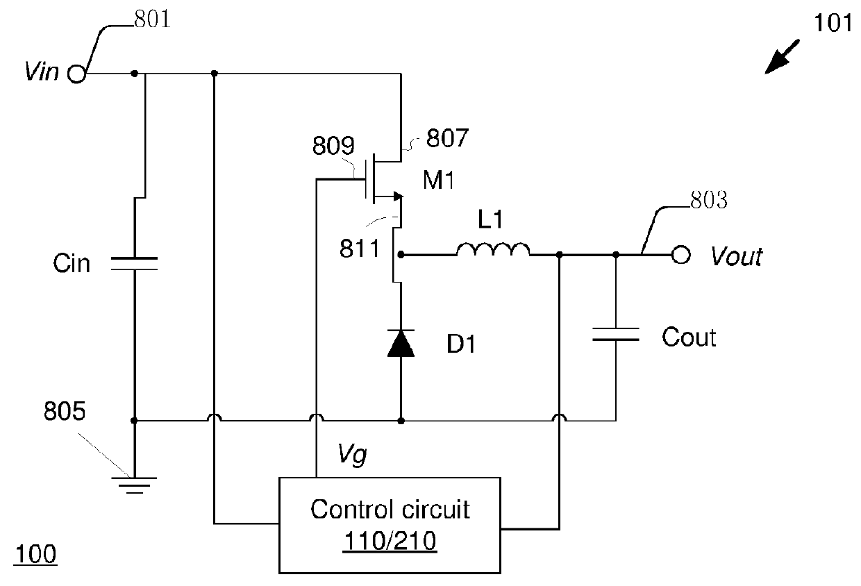
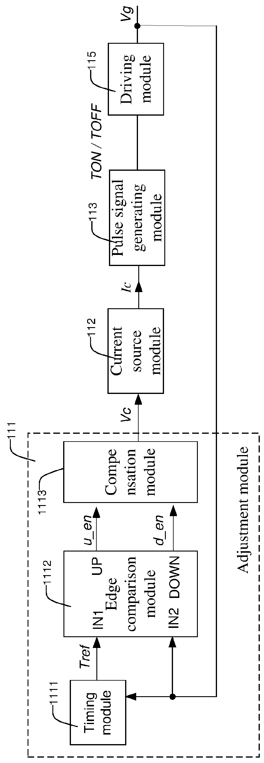
[0114]FIG. 7 is a schematic block diagram of a control circuit 210 of the switch power supplies 100 / 200 according to the disclosure. As shown in FIG. 7, the control circuit 210 includes an adjustment module 211, a current source module 212, a pulse signal generating module 213, a time measurement module 214 and a drive module 215. The adjustment module 211 generates the control voltage Vc based on the switch signal Vg. The current source module 212 produces the charging current Ic according to the control voltage Vc. In constant on time control mode, the pulse signal generating module 213 generates the switch turn-on signal TON in accordance with the charging current Ic. The drive module 215 produces the switch signal Vg based on the switch turn-on signal TON.
[0115]The structure and function of the current source module 212, the pulse signal generating module 213 and drive module 215 of the switch power supply control circuit in this embodiment are the same as the current source mod...
second embodiment
[0142]FIG. 10 is a flow chart of a constant on time control method of the switch power supply according to the disclosure. In this embodiment, the control method is realized by using the control circuit 210 shown in FIG. 7 and the timing module 2111 shown in FIG. 8 after the switch power supply 100 / 200 is powered on. The control method performs some but not all of the functions of the control circuit 210.
[0143]In step S101, the off time Tf of the switch signal Vg is detected.
[0144]In step S102, the control circuit 210 decides whether the off time Tf of the switch signal is smaller than the first threshold Tth1. For example, the first threshold Tth1 corresponds to the minimum off time Tf_min of the system. If the off time Tf of the switch signal Vg is smaller than the first threshold Tth1, step S105 is executed, and if the off time Tf of the switch signal Vg is greater than or equal to the first threshold Tth1, step S104 is executed.
[0145]In step S104, the current of the current sour...
third embodiment
[0148]FIG. 11 is a flow chart of a constant on time control method of the switch power supply according to the disclosure. In this embodiment, the control method is realized by using the control circuit 210 shown in FIG. 7 and the timing module 2111 shown in FIG. 8 after the switch power supply 100 / 200 is powered on. The control method performs some but not all of the functions of the control circuit 210.
[0149]The steps S201, S202, S205 and S206 of the switch power supply control method in this embodiment are the same as the corresponding steps S101, S102, S105 and S106 of control method shown in FIG. 10. The difference of the two is described below.
[0150]In step S202, the control circuit 210 decides whether the off time Tf of the switch signal is smaller than the first threshold Tth1. For example, the first threshold Tth1 corresponds to the minimum off time Tf_min of the system. If the off time Tf of the switch signal Vg is smaller than the first threshold Tth1, step S205 is execut...
PUM
 Abstract
Description
Claims
Application Information


