Microfabricated optical apparatus with flexible electrical connector

a technology of flexible electrical connectors and optical apparatuses, applied in the field of microfabricated optical apparatuses, can solve problems such as limiting high speed performance, and achieve the effects of reducing capacitive coupling, increasing device density, and reducing manufacturing costs

Inactive Publication Date: 2018-06-28
INNOVATIVE MICRO TECH
View PDF6 Cites 10 Cited by
  • Summary
  • Abstract
  • Description
  • Claims
  • Application Information

AI Technical Summary

Benefits of technology

[0012]Numerous devices can make use of the systems and methods disclosed herein. In particular, high speed, compact telephone or communications switching equipment may make use of this architecture. RF switches benefit from the reduced capacitive coupling that an insulative substrate can provide. High density vias formed in the insulative substrate increase the density of devices which can be formed on a substrate, thereby reducing cost to manufacture. Other sorts of substrates, for example, metal or semiconducting substrates may make use of an insulating layer to provide isolation between the conductive via and the surrounding substrate. The performance of such devices may also be improved, in terms of insertion loss, distortion and isolation figures of merit.

Problems solved by technology

Because the enclosed elements may be delicate, the bondlines may be, for example, metal alloy bondlines that are activated at relatively low processing temperatures.
However, the presence of the flat metal bondlines directly adjacent to potentially high frequency signal lines may cause unwanted capacitance in the structure, limiting its high speed performance.

Method used


Image

  • Microfabricated optical apparatus with flexible electrical connector
  • Microfabricated optical apparatus with flexible electrical connector
  • Microfabricated optical apparatus with flexible electrical connector

Examples


first embodiment

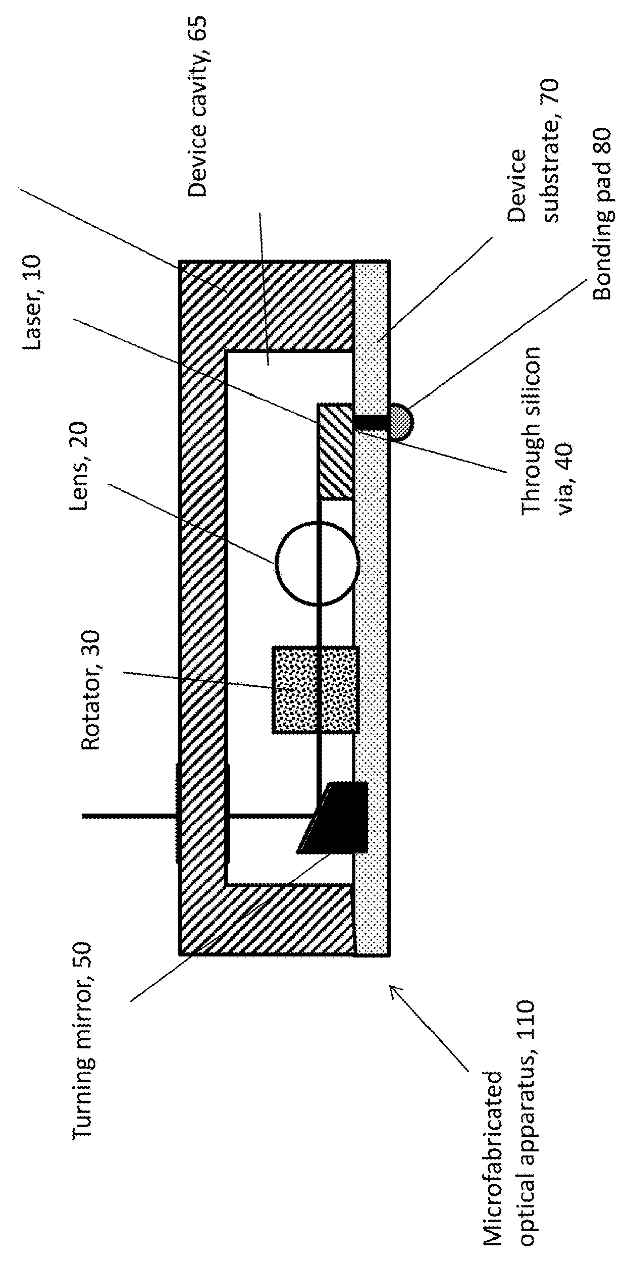
[0043]FIG. 1 shows the systems and methods disclosed here. In FIG. 1, there may be a laser light source 10 which produces a beam of light which may be shaped by a ball lens 20 and then through Faraday rotator 30. The beam of light then impinges on a turning surface 50 which redirects the light in a direction normal to the substrate, shown upward in FIG. 1. The light may pass through the lid substrate 60 which may encapsulate the aforementioned devices disposed on the device substrate 70. In FIG. 1, the turning surface is a turning mirror 50, which is a discrete structure, encapsulated in the device cavity along with the other components.

[0044]Suitable materials for the device substrate 70 and lid substrate 60 may be a metal or semiconductor such as silicon, or a ceramic or glass. The device cavity 65 may be etched into the lid wafer 60 using, for example, deep reactive ion etching (DRIE). The depth of the device cavity may be several hundred microns and have sufficient lateral exten...

second embodiment

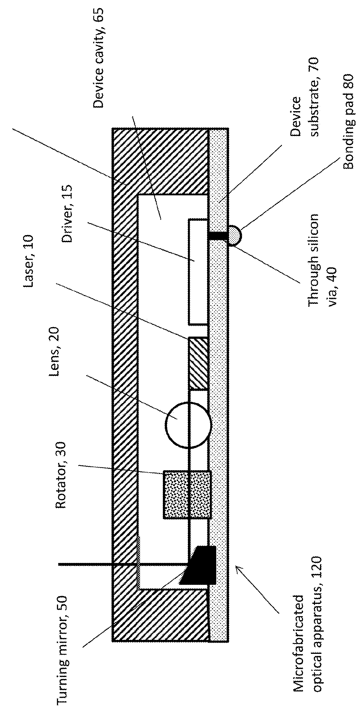
[0047]FIG. 2 shows another embodiment of the MEMS silicon optical apparatus. This second embodiment is similar to that shown in FIG. 1, except that in this embodiment, there is also a driver 15 that drives the laser 10 with a particular pattern or modulation that may represent data to be communicated over the optical link. Like the previous embodiment, there is once again a laser light source 10, which produces a beam of light which may be shaped by a ball lens 20, and then modulated by a Faraday rotator 30. The beam of light then impinges on a turning surface 50 which redirects the light in a direction normal to the substrate, shown as upward in FIG. 3. The light may pass through the lid substrate 60 which encapsulates the aforementioned devices disposed on the device substrate 70. In FIG. 2, the turning surface is a turning mirror 50, which is a discrete structure, encapsulated in the device cavity along with the other components. As in the previous embodiment, the laser is driven...

third embodiment

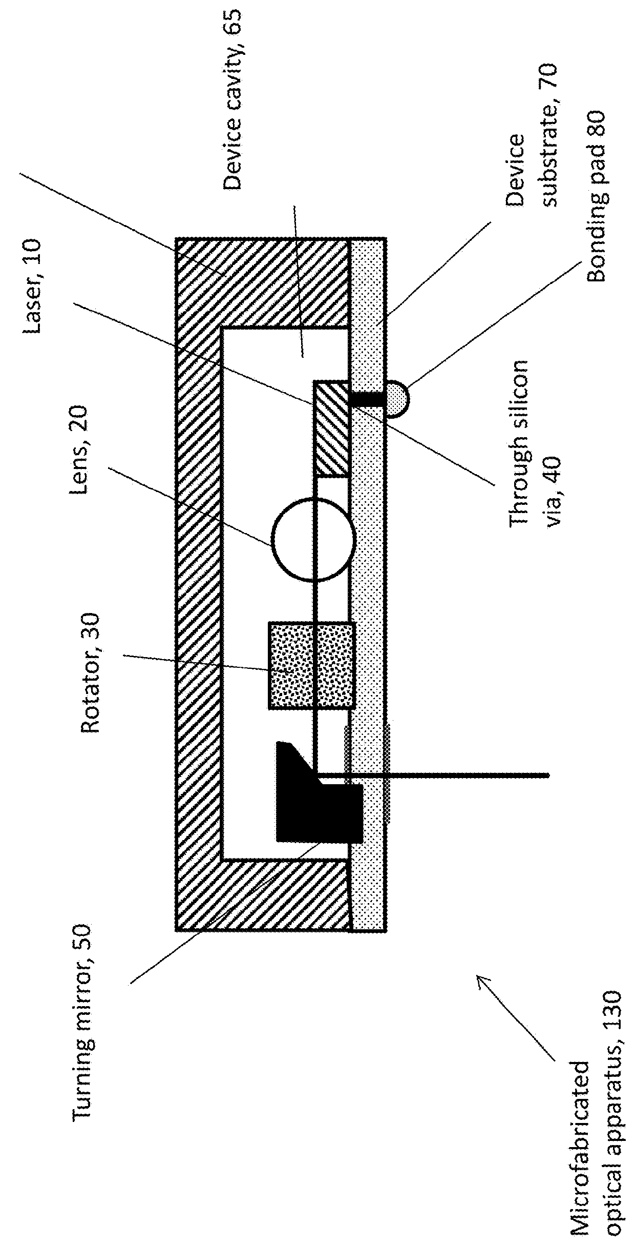
[0049]FIG. 3 shows a third embodiment, wherein the turning mirror 50 directs the beam of light downward through the device substrate 70 rather than upward through the lid wafer 60. As in the previous embodiments, the laser may be driven by through substrate vias 40, which may improve the high frequency characteristics of the device. The output of this embodiment may be generally downward on the same side of the device as the electrical connections are made. Accordingly, in contrast to the embodiment shown in FIGS. 2 and 3, the optical apparatus in FIG. 3 has a turning mirror 50 which may bend the optical radiation to exit the device cavity through the device substrate 70, in a substantially parallel direction relative to the through silicon via.


PUM

PropertyMeasurementUnit
depthaaaaaaaaaa
wavelengthsaaaaaaaaaa

Abstract

A microfabricated optical apparatus that includes a light source driven by a waveform, wherein the waveform is delivered to the light source by at least one through silicon via. The microfabricated optical apparatus may also include a light-sensitive receiver which generates an electrical signal in response to an optical signal. An optical source may be attached to a carrier substrate with the TOSA by a flexible connector, in order to align the optical source before affixing it permanently.

Description

CROSS REFERENCE TO RELATED APPLICATIONS[0001]Not applicable.STATEMENT REGARDING FEDERALLY SPONSORED RESEARCH[0002]Not applicable.STATEMENT REGARDING MICROFICHE APPENDIX[0003]Not applicable.BACKGROUND[0004]This invention relates to integrated circuit and microelectromechanical systems (MEMS) devices. More particularly, this invention relates to a microfabricated optical apparatus wherein vias are formed completely through the silicon substrates.[0005]Microelectromechanical systems (MEMS) are very small moveable structures made on a substrate using lithographic processing techniques, such as those used to manufacture semiconductor devices. MEMS devices may be moveable actuators, sensors, valves, pistons, or switches, for example, with characteristic dimensions of a few microns to hundreds of microns. One example of a MEMS device is a microfabricated cantilevered beam, which may be used to switch electrical signals. Because of its small size and fragile structure, the movable cantileve...

Claims


Application Information

Patent Timeline
Patent Type & Authority Applications(United States)
IPC IPC(8): G02B6/42G02F1/095B81C1/00B81B7/00G02B27/09H01S5/183H01S5/02H01S5/022H04J14/02H04B10/40
CPCG02B6/4284G02F1/0955B81C1/00301B81B7/0067B81B7/007G02B27/0955H01S5/18361H01S5/021H01S5/02284H01S5/02288H01S5/02252H01S5/02292H04J14/02H04B10/40H01S5/0064H01S5/02216H01S5/4025G02B6/4213G02B6/4214G02B6/4246G02B6/4257H04B10/508B81B7/02B81B2201/042B81B2201/047B81B2207/015B81B2207/096H01S5/02326H01S5/02325H01S5/02255H01S5/02257H01S5/02253H01S5/02251
Inventor GUDEMAN, CHRISTOPHER S.
Owner INNOVATIVE MICRO TECH
Why Eureka
Try Eureka