Method of manufacturing semiconductor device

Active Publication Date: 2018-06-28
NTT MOBILE COMM NETWORK INC
View PDF1 Cites 1 Cited by
  • Summary
  • Abstract
  • Description
  • Claims
  • Application Information

AI Technical Summary

Benefits of technology

[0006]Described herein is a technique capable of forming a side wall of a

Problems solved by technology

When over-etching occurs, the sidewall becomes thinner and the leakage current increases.
However, since the

Method used


Image

  • Method of manufacturing semiconductor device
  • Method of manufacturing semiconductor device
  • Method of manufacturing semiconductor device

Examples


Example

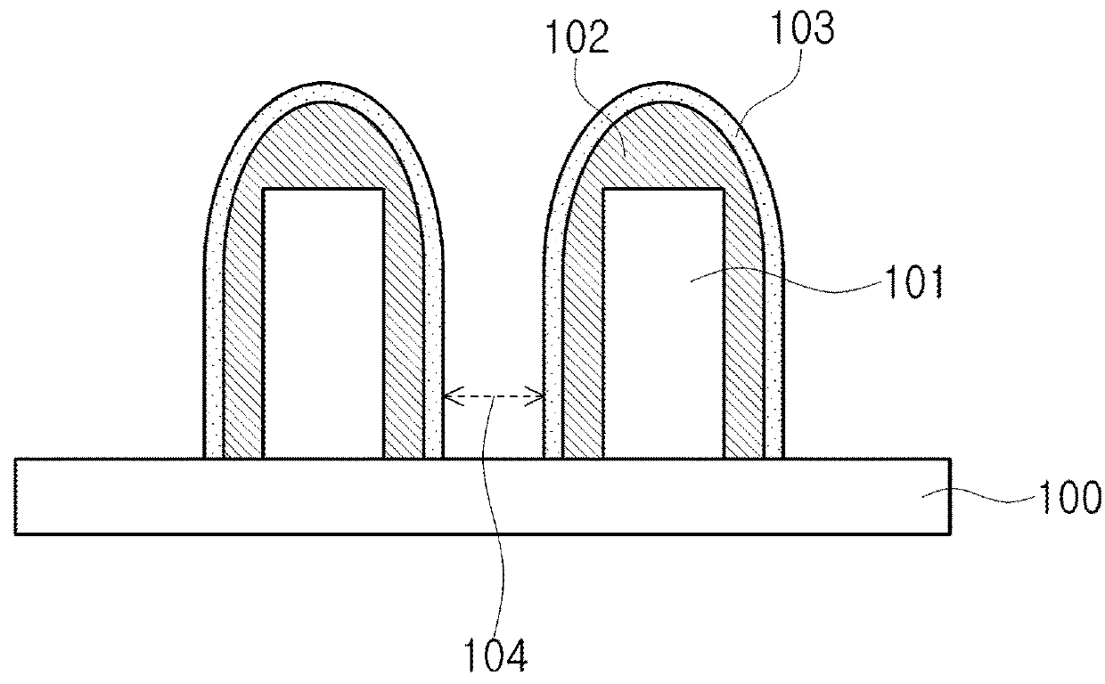
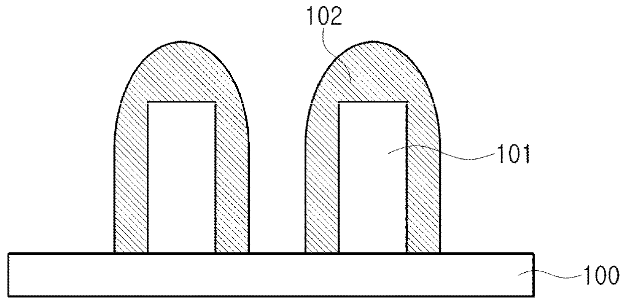
[0017]A first embodiment will be described below. First, a substrate 100 to be processed according to the first embodiment will be described with reference to FIG. 1. A gate electrode 101 is formed on the substrate 100. The gate electrode 101 includes a film such as titanium nitride (TiN) film and tungsten (W) film. An insulating film 102, which is later etched to be a side wall, is formed on surface of the gate electrode 101. The insulating film 102 may include a silicon nitride (SiN) layer.

[0018]The insulating film 102 is formed so as not to include a carbon component. For example, the insulating film 102 includes a silicon nitride layer free of carbon, which is also referred to as a carbon-free silicon nitride layer. Since the insulating film 102 is free of carbon, the insulating film 102 does not contribute to an increase in leakage current.

[0019]Next, an etching-resistant film 103 according to the first embodiment will be described with reference to FIG. 2. In the carbon-contai...

Example

Second Embodiment

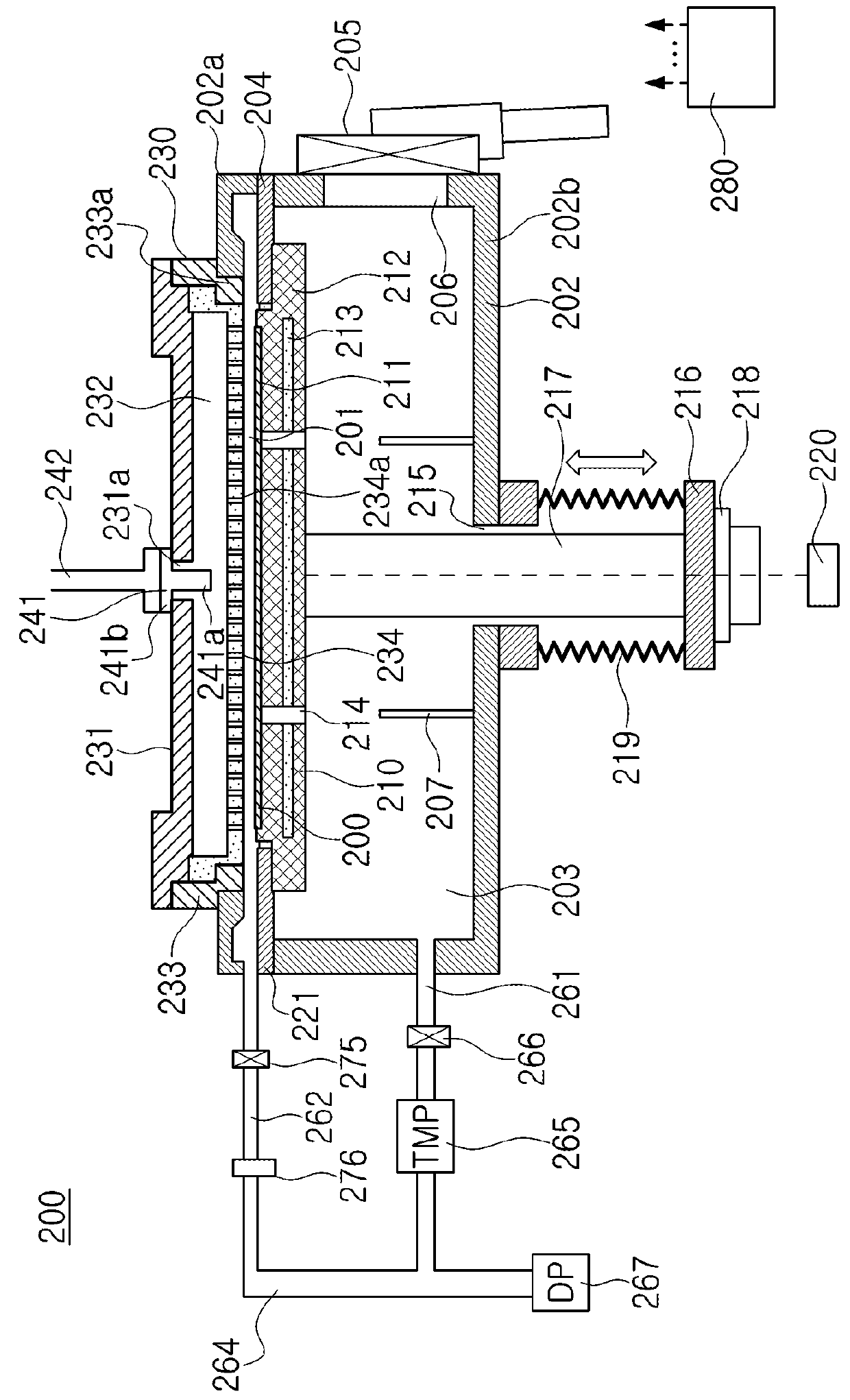
[0064]Next, a second embodiment will be described with reference to FIGS. 7 and 8. FIG. 7 schematically illustrates a gas supply system of a substrate processing apparatus according to the second embodiment, and FIG. 8 schematically illustrates a flow of a substrate processing according to the second embodiment. The configuration of the second embodiment differs from that of the first embodiment in that the substrate processing apparatus according to the second embodiment further includes a second gas supply system and a third gas supply system and the substrate processing according to the second embodiment further includes a nitrogen-containing gas supply step.

[0065]Hereinafter, the second embodiment will be described in detail. The configuration of the second embodiment the same as that of the first embodiment is omitted.

Second Gas Supply System

[0066]A second gas supply system 244 may also be referred to as a second gas supply unit. A second gas supply source 244b...

Example

Third Embodiment

[0083]Next, a third embodiment will be described with reference to FIG. 9. The configuration of the third embodiment differs from that of the first embodiment in that a substrate processing apparatus 200′ of the third embodiment further includes a structure capable of generating plasma directly in the processing space 201. Specifically, the substrate processing apparatus 200′ shown in FIG. 9 further includes a plasma generation unit 250. According to the third embodiment, the substrate support 212 of the substrate processing apparatus 200′ is electrically grounded.

[0084]The plasma generation unit 250 may include a matching unit 251 and a power supply 252. One electrode of the power supply 251 is connected to the matching unit 252, and the other electrode of the power supply 251 is electrically grounded. That is, the power supply 251 is electrically connected to the dispersion plate 234 via a matching unit 252. The dispersion plate 234 is disposed adjacent to the uppe...


PUM

PropertyMeasurementUnit
Electrical resistanceaaaaaaaaaa
Ratioaaaaaaaaaa

Abstract

A technique capable of forming a side wall of a gate electrode having high resistance-to-etching and low leakage current is provided. A method of manufacturing a semiconductor device according to the technique includes: (a) loading a substrate into a processing space in a process vessel, the substrate having thereon a gate electrode and an insulating film formed on a side surface of the gate electrode as a side wall; and (b) forming an etching-resistant film containing carbon and nitrogen on a surface of the insulating film by supplying a carbon-containing gas into the processing space.

Description

CROSS-REFERENCE TO RELATED PATENT APPLICATION[0001]This U.S. non-provisional patent application claims priority under 35 U.S.C. § 119 of Japanese Patent Application No. 2016-255033, filed on Dec. 28, 2016, in the Japanese Patent Office, the entire contents of which are hereby incorporated by reference.BACKGROUND1. Field[0002]The present disclosure relates to a method of manufacturing a semiconductor device.2. Description of the Related Art[0003]Recently, semiconductor devices are integrated at high density. As a result, the distance between electrodes or between wirings is reduced. Accordingly, the electrical capacitance between the electrodes or between the wirings increases.[0004]Generally, the leakage current increases as the electrical capacitance increases. In view of the efficiency of the semiconductor device, the increase in the leakage current is not preferable. Therefore, for example, by forming sidewalls made of insulating material around the electrodes, leakage current is...

Claims


Application Information

Patent Timeline
IPC IPC(8): H01L21/02H01L21/673C23C16/34C23C16/50C23C16/32
CPCH01L21/02167H01L21/0217H01L21/67389C23C16/345C23C16/50C23C16/325H01L21/67778H01L21/67383H01L21/285H01L21/67011C23C16/36H01L21/02321H01L21/02329H01L21/0234H01L21/3115H01L21/68742H01J37/32449H01J37/32834H01J37/32357H01J37/3244H01L21/02274H01L21/28132H01L21/67017H01L21/683H01L21/76852
Inventor OGAWA, ARITOHIYAMA, SHIN
Owner NTT MOBILE COMM NETWORK INC
Why Eureka
Try Eureka