

Method of producing semiconductor chip, and mask-integrated surface protective tape used therein
- Summary
- Abstract
- Description
- Claims
- Application Information
AI Technical Summary
Benefits of technology
Problems solved by technology
Method used
Image

Examples
example 1
[Example 1] Production of Semiconductor Chip-1
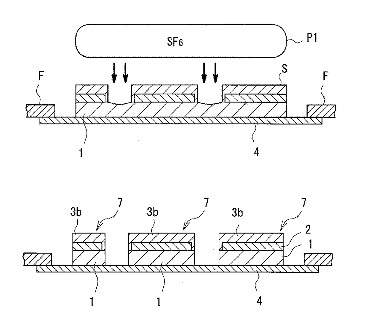
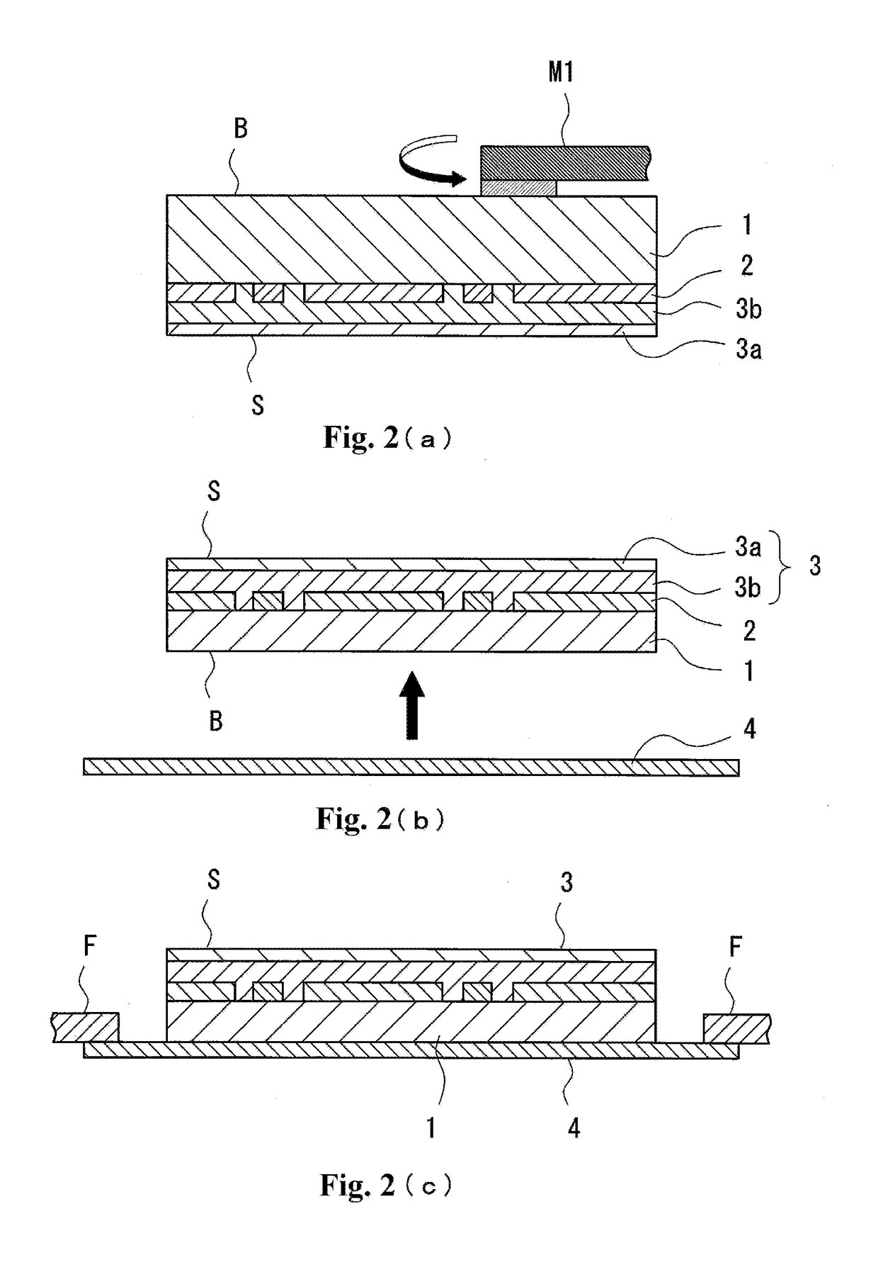
[0124]The obtained mask-integrated surface protective tape 3 was laminated on a silicon wafer (diameter: 8 inches) using a tape laminator (trade name: DR-300011, manufactured by Nitto Seiki Co., Ltd.). The wafer laminated with the mask-integrated surface protective tape 3 was ground until the thickness of 50 μm using a backgrinding apparatus (trade name: DGP8760, manufactured by Disco Corporation). The presence or absence of the crack in the wafer at that time was determined visually and also by using a microscope.
[0125]An UV-curable wafer fixing tape 4 (trade name: UC-353EP-110, manufactured by Furukawa Electric Co., Ltd.) was laminated on the ground wafer backing-face side, followed by supporting and fixing by using the ring flame. Next, an ultraviolet light was irradiated from the side of the mask-integrated surface protective tape 3, and then the surface protective tape 3a was peeled off, leaving the mask material layer 3b. And by ir...
example 2
[Example 2] Production of Semiconductor Chip-2
[0128]Semiconductor chips were obtained in the same manner as in Example 1, except that as the mask-integrated surface protective tape 3 in Reference Example 1, the mask-integrated surface protective tape prepared in Reference Example 2 was used in place of the mask-integrated surface protective tape prepared in Reference Example 1.
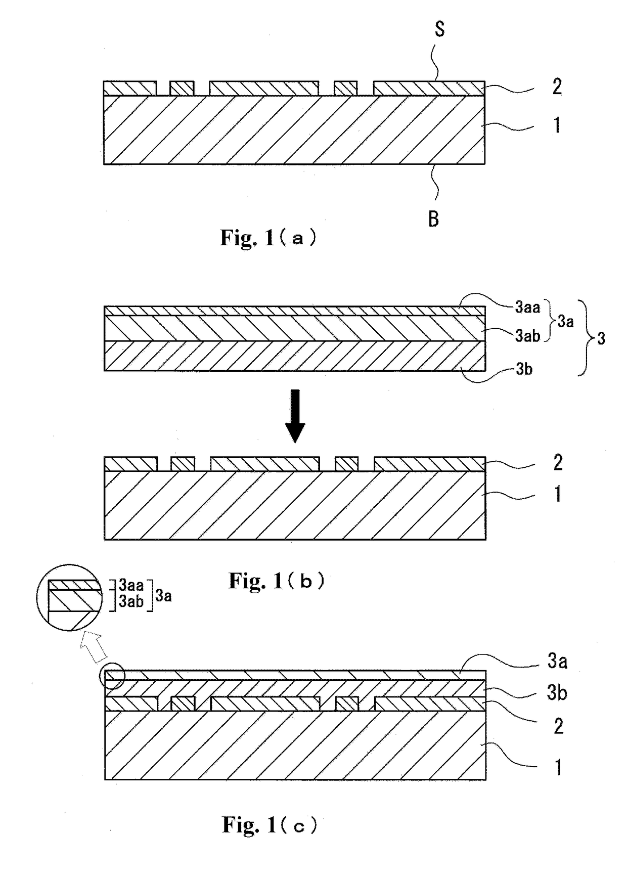
[Reference Example 3] Preparation of Mask-Integrated Surface Protective Tape-3
[0129]A mask-integrated surface protective tape was obtained in the same manner as in Reference Example 1, except that PET (polyethylene terephthalate) film having a thickness of 50 μm was used in place of the substrate film having a structure of 2 layers composed of LDPE and EVA as the substrate film 3aa in Reference Example 1.
example 3
[Example 3] Production of Semiconductor Chip-3
[0130]Semiconductor chips were obtained in the same manner as in Example 1, except that as the mask-integrated surface protective tape 3 in Reference Example 1, the mask-integrated surface protective tape prepared in Reference Example 3 was used in place of the mask-integrated surface protective tape prepared in Reference Example 1.
[Reference Example 4] Preparation of the Mask-Integrated Surface Protective Tape-4
[0131]A mask-integrated surface protective tape was obtained in the same manner as in Reference Example 1, except that a single layer film (thickness: 100 μm) of EVA resin (ULTRATHENE 510, manufactured by Tosoh Corporation) was used in place of the substrate film having a structure of 2 layers composed of LDPE and EVA as the substrate film 3aa in Reference Example 1.
PUM
| Property | Measurement | Unit |
|---|---|---|
| Percent by mass | aaaaa | aaaaa |
| Length | aaaaa | aaaaa |
| Nanoscale particle size | aaaaa | aaaaa |
Abstract
Description
Claims
Application Information