Process and material for growth of adsorbed compound via nanoscale-controlled resistive heating and uses thereof

a technology of resistive heating and nanoscale, which is applied in the direction of catalyst activation/preparation, metal/metal-oxide/metal-hydroxide catalyst, synthetic resin layered products, etc., can solve the problem of material decomposition in air, and achieve the effect of reducing the number of components needed to produce nanostructured materials, reducing costs, and increasing control of nanostructur

Active Publication Date: 2018-07-05
SABIC GLOBAL TECH BV
View PDF6 Cites 5 Cited by
  • Summary
  • Abstract
  • Description
  • Claims
  • Application Information

AI Technical Summary

Benefits of technology

[0008]A solution to the problems associated with the preparation of nanoscale and microscale materials for commercial use (e.g. catalytic material, electronic devices, optical devices, sensing devices, piezoelectrical materials, etc.) has been discovered. The solution is premised on combining (1) the use of resistive heating to produce nanostructured material directly onto an electrically conductive layer of micro- and / or nanostructures and (2) sufficient attachment of the electrically conductive layer to a substrate by embedding the conductive layer into the substrate prior to producing the catalytic material. One advantage of this process is that it can reduce the costs associated with making materials that can be used in various applications (e.g., catalysts used in chemical reactions, materials that can be incorporated into electronic devices, etc.). In particular, depositing the precursor material directly onto the embedded conductive micro- and / or nanostructures allows for a more facile production process, as the number of components needed to produce the nanostructured material is reduced. Further, the direct deposition of the precursor material onto the embedded micro- and / or nanostructures combined with localized resistive heating allows for an increased control of the nanostructure, metal particle size, and or particle / cluster size distribution. By way of example, in instances where a multi-layered catalyst is desired (e.g., bi-metallic catalysts), the processes of the present invention can be used to deposit the desired metals in a desired order to obtain a specific structure (e.g., Pt / Ni bimetallic catalysts, Pt / Co bimetallic catalysts, etc.). For instance, the metals can be evaporated / deposited onto the micro- or nanostructure in an order of A-B-A, wherein A is one metal, and B is a second metal. In general, different lattice structures, different layers, different metals or metal oxides altogether can be easily produced with the processes of the present invention.

Problems solved by technology

This conventional technique can result in decomposition of material in air.

Method used


Image

  • Process and material for growth of adsorbed compound via nanoscale-controlled resistive heating and uses thereof
  • Process and material for growth of adsorbed compound via nanoscale-controlled resistive heating and uses thereof
  • Process and material for growth of adsorbed compound via nanoscale-controlled resistive heating and uses thereof

Examples


example 1

Preparation of Supported Material Containing Joule Heaters

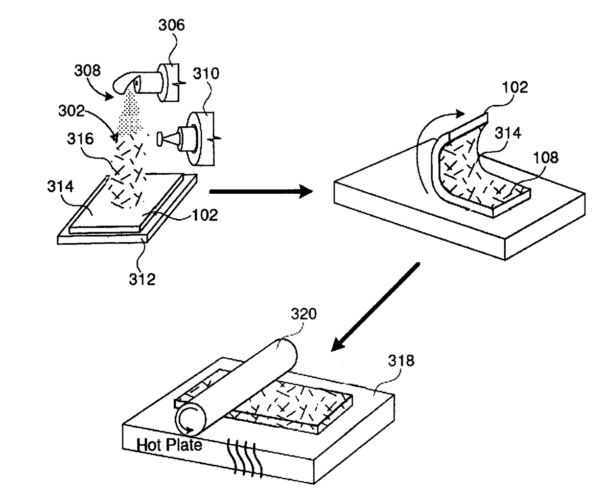
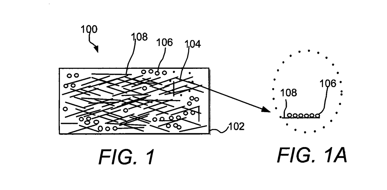
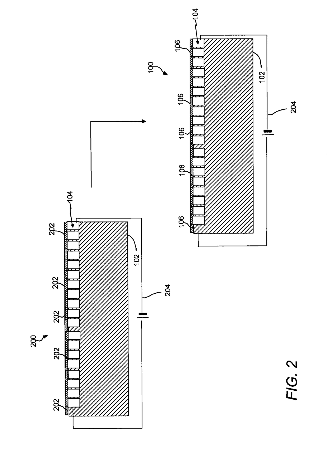
[0103]Supported material containing joule heaters were fabricated by putting a droplet of silver paint on copper wire placed at the edge of the polycarbonate film sheets (1.6 cm×0.3 cm) containing joule heaters made by embedding sliver nanowires (Ag NW) in the surface of the film. The heaters had a resistance of about 30-35 Ω / square). The electrode dimensions were kept fixed for all the experiments. A multi-meter was used to check the resistance of the electrode. DC voltage was applied to the film heater through a copper contact at the film edge and the current and resistance were monitored.

example 2

Formation of Nanostructures on a Supported Material

[0104]A droplet of nanostructure precursor a salt solution (2-5 μL, H2PtCl6 (1.95×10⁻⁴ M), TEOS, 99%, or zinc acetate (0.01 M in water)) was deposited on the supported material prepared as described in Example 1, which was connected to the DC power supply. The droplet did not dry during the experiment. The DC voltage ranging between 0.6 V and 6 V was applied (the voltage was raised to the desired value in steps of 0.2-0.3 V) for 1 hr. Three voltages were selected (2 V, 3.6 V, and 4.8 V) and joule heating of the salt was conducted for a specific duration (5 min, 10 min, 20 min, 40 min, and 60 min) at each voltage to convert the nanostructure precursor to a nanostructure (e.g., zinc acetate liquid to zinc oxide nanostructures, chloroplatinic acid to platinum nanostructures, and tetraethyl orthosilicate to silica nanostructures). Short nanowires had a length of 10 to 20 microns and long nanowires had a length of 30 to 40 microns

example 3

Characterization of Nanostructures

[0105]The supported structures containing the nanostructures were analyzed for morphology, size, and composition using scanning electron microscopy (SEM) and energy dispersive spectroscopy (EDS) using a JSM 7800F Prime (JEOL, U.S.A.)

[0106]1. Zinc Oxide Nanostructures in Polycarbonate Polymer Matrix

[0107]Different shapes of zinc oxide nanostructures evolved (cross-sections: circular, triangular, hexagonal, pentagonal, rectangular, rhombus, etc.) as a function of joule heating voltage and duration. FIG. 11 shows includes Table 2, which lists the conditions for forming the nanostructures from zinc acetate at a 1 hour duration time period, and a schematic of the types of nanostructures formed. FIG. 12 shows the EDS of the zinc acetate precursor decomposition to zinc oxide. FIG. 13 shows different SEM images of the zinc oxide nanoparticles formed from zinc acetate at 0.6 V, 1.2 V, 1.8 V, 2.0 V, 2.4 V, 2.5 V, 3.0 V, 3.6 V, 4.2 V, 4.8 V, 5.4 V, and 6.0 V u...


PUM

PropertyMeasurementUnit
speedaaaaaaaaaa
speedaaaaaaaaaa
speedaaaaaaaaaa

Abstract

Disclosed is a method for making a material having supported micro- and/or nanostructures, the method includes (a) obtaining a substrate comprising a precursor material and an electrically conductive layer of micro- or nanostructures embedded into at least a portion of a first surface of the substrate, and (b) applying a voltage across the electrically conductive layer to heat the micro- or nanostructures, wherein the heat converts the precursor material into micro- and/or nanostructures.

Description

CROSS REFERENCE TO RELATED APPLICATIONS[0001]This application claims priority to U.S. Provisional Patent Application No. 62 / 188,087 filed Jul. 2, 2015, and U.S. Provisional Patent Application No. 62 / 355,073 filed Jun. 27, 2016. The entire contents of each of the above-referenced disclosures are specifically incorporated herein by reference without disclaimer.BACKGROUND OF THE INVENTIONA. Field of the Invention[0002]The invention generally concerns a process for making materials having micro- or nanostructures that can be used in a wide-array of applications (e.g., chemical, electrical, optical, sensing, piezoelectrical, etc., applications). In particular, the process can include the use of resistive heating (e.g., with applied voltage) of an electrically conductive layer of micro- or nanostructures doped with, or in the presence of, a precursor material to obtain the nanostructured material. The electrically conductive layer is embedded into a substrate, thereby allowing for the cre...

Claims


Application Information

Patent Timeline
Patent Type & Authority Applications(United States)
IPC IPC(8): C08J7/06C08K3/22C08K3/08C08K3/36C10G35/06B01J31/06B01J23/06B01J23/42B01J21/08B01J35/00B01J37/34C08J7/043C08J7/044
CPCC08J7/06C08K3/22C08K3/08C08K3/36C10G35/06B01J31/06B01J23/06B01J23/42B01J21/08B01J35/0006B01J35/0013B01J35/0033B01J37/348C08K2003/2296C08K2201/001C08K2201/011C08J2369/00C08J2379/08C10G2300/708B82Y40/00B32B27/00Y02E60/10H01M50/446C08J7/043C08J7/044
Inventor ODEH, IHAB N.CHOPRA, NITINAL-HUSSAIN, SAAD
Owner SABIC GLOBAL TECH BV
Why Eureka
Try Eureka