

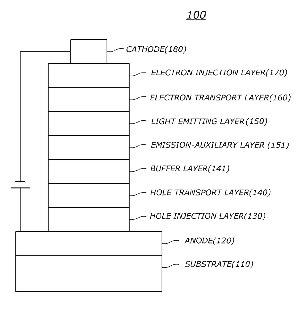
Organic electric element comprising compound for organic electric element and electronic device thereof
a technology of organic electric elements and compounds, which is applied in the direction of organic chemistry, luminescent compositions, chemistry apparatuses and processes, etc., can solve the problems of power consumption increasing and more, efficiency and life span issues also need to be solved, and the efficiency cannot be maximized, so as to achieve high heat resistance, low driving voltage, and high luminous efficiency
- Summary
- Abstract
- Description
- Claims
- Application Information
AI Technical Summary
Benefits of technology
Problems solved by technology
Method used
Image


Examples
synthesis example
of Sub 1-A29
[0164]1-bromo-4-iodobenzene (7.26 g, 25.7 mmol), Pd(PPh3)4 (0.99 g, 0.9 mmol), K2CO3 (7.1 g, 51.3 mmol), THF, water were added to Sub 1-VI-A29 (9.61 g, 17.1 mmol) obtained in the above synthesis, and then 8.09 g (yield: 80%) of the product was obtained by using the same manner as described above for the synthesis example of Sub 1-A1.
(6) Synthesis Example of Sub 1-A35
[0165]
[0166]Synthesis of Intermediate Sub 1-III-A35
[0167]2-bromo-9,9-diphenyl-9H-fluorene (154.31 g, 388.4 mmol), Na2SO4 (36.78 g, 258.9 mmol), K2CO3 (35.79 g, 258.9 mmol), Cu (4.94 g, 77.7 mmol), nitrobenzene were added to Sub 1-II-A1 (63.72 g, 258.9 mmol) obtained in the above synthesis, and then 88.84 g (yield: 61%) of the product was obtained by using the same manner as described above for the synthesis example of Sub 1-III-A1.
[0168]Synthesis of Intermediate Sub 1-IV-A35
[0169]Bis(pinacolato)diboron (44.12 g, 173.7 mmol), Pd(dppf)Cl2 (3.87 g, 4.7 mmol), KOAc (46.5 g, 473.8 mmol), DMF were added to Sub 1-II...
synthesis example 2
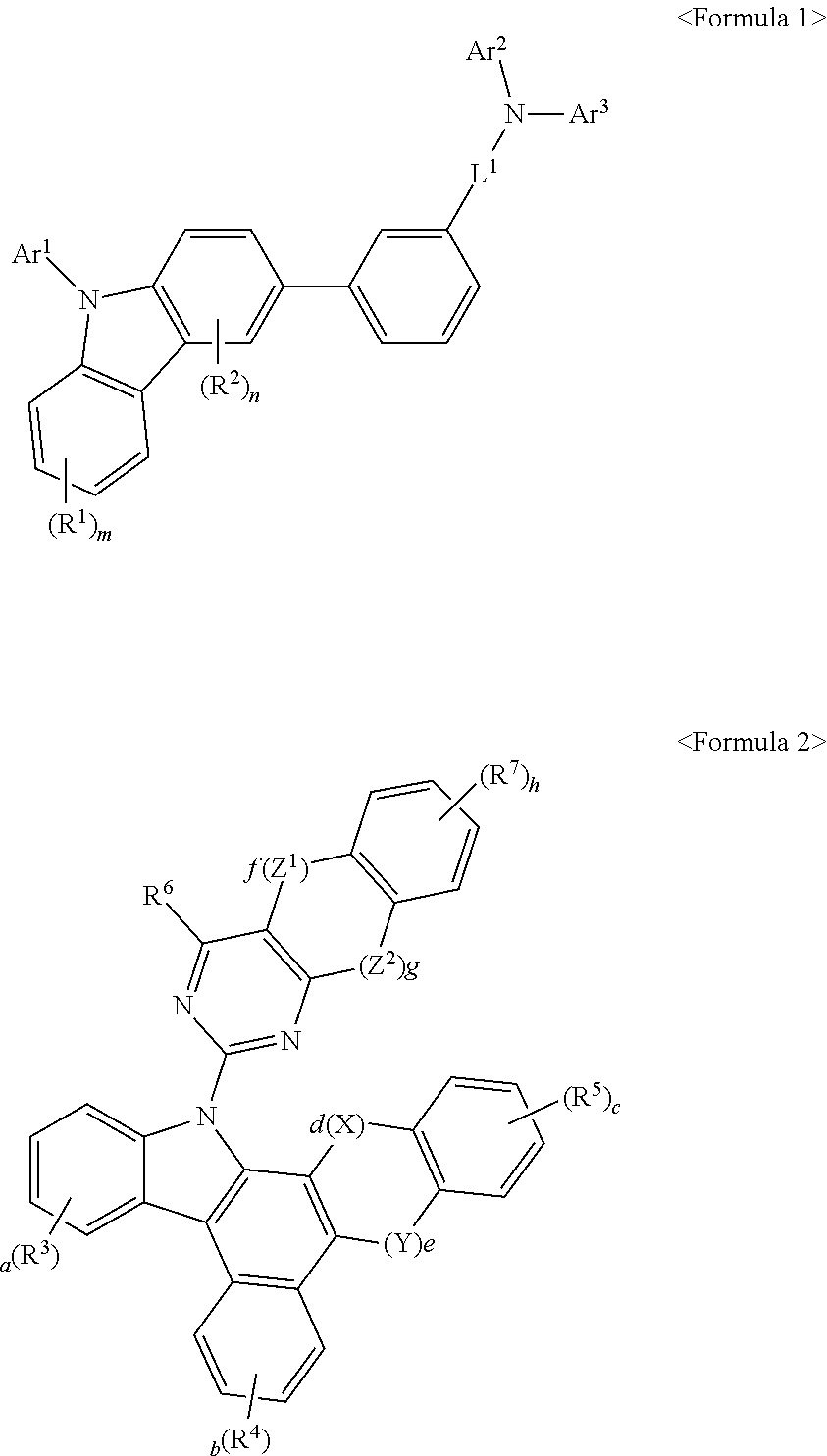
[0325]The compound(final products) represented by Formula 2 according to the present invention are synthesized by reacting Sub 3 and Sub 4 as shown in Reaction Scheme 65, but are not limited thereto.
[0326]I. Synthesis of Sub 3
1. Synthesis Example of 3-1 Core
[0327]
Synthesis Example of 3-1-C1
[0328]5-bromobenzo[b]naphtha[1,2-d]thiophene (50 g, 0.16 mol), bis(pinacolato)diboron (48.65 g, 0.19 mol), KOAc (47 g, 0.48 mol), PdCl2(dppf) (5.21 g, 4 mol %) were dissolved in DMF solvent in a round bottom flask, and then refluxing at 120° C. for 12 hours was followed. When the reaction was completed, the reaction product is cooled to room temperature, was extracted with CH2Cl2 and was washed with water. Then, the organic layer was dried with MgSO4 and concentrated, and recrystallization of the concentrate was carried out using CH2Cl2 and a methanol solvent to obtain the desired 3-1-C1 (46 g, 80%).
Synthesis Example of 3-1-C2
[0329]3-1-C1 (40 g, 0.11 mol), bromo-2-nitrobenzene (26.91 g, 0.13 mol),...
synthesis example 3
[0458]Final products represented by Formula 8 according to the present invention are synthesized by reacting Sub 5 or Sub 6 and Sub 2 as shown in Reaction Scheme 2, but are not limited thereto.
[0459](L is L2 to L4 defined in formulas 8-1, 8-2 and 8-3, Ar is Ar4, Ar5)
1. Synthesis Example of Sub 5
[0460]
[0461]Here, S1 to S7 are as follows.
1) Synthesis Example of Sub 5-1-1 (L=biphenyl)
[0462]
[0463]The starting material 9H-carbazole (50.16 g, 300 mmol) was dissolved in nitrobenzene (600 ml), and then, 4-bromo-4′-iodo-1,1′-biphenyl (129.2 g, 360 mmol), Na2SO4 (42.6 g, 300 mmol), K2CO3 (41.4 g, 300 mmol), Cu (5.72 g, 90 mmol) were added and stirred at 200° C. When the reaction was completed, nitrobenzene was removed by distillation, and then the reaction product was extracted with CH2Cl2 and water. Then, the organic layer was dried with MgSO4 and concentrated, and the concentrate was passed through silica gel column and recrystallized to obtain 80.05 g (yield: 67%) of the product.
2) Synthes...
PUM
| Property | Measurement | Unit |
|---|---|---|
| thickness | aaaaa | aaaaa |
| thickness | aaaaa | aaaaa |
| thickness | aaaaa | aaaaa |
Abstract
Description
Claims
Application Information