OLED light-emitting device, production method thereof and display apparatus

a light-emitting device and light-emitting technology, applied in the field of oled display, can solve the problems of restricting the internal quantum efficiency of the device from the material aspect, and achieve the effects of reducing the quenching of triplet-triplets, enhancing the speed of spontaneous radiation of triplet excitons, and high current density

Active Publication Date: 2018-07-26
BOE TECH GRP CO LTD +1
View PDF5 Cites 5 Cited by
  • Summary
  • Abstract
  • Description
  • Claims
  • Application Information

AI Technical Summary

Benefits of technology

[0005]This disclosure provides an OLED light-emitting device and a production method thereof as well as a display apparatus, which can enhance the internal quantum efficiency of a blue OLED light-emitting device.
[0022]An embodiment of the disclosure provides an OLED light-emitting device. By forming an Ag nanolayer between the anode and the hole transport layer, enabling the absorption spectrum of the Ag nanolayer to overlap the emission spectrum of the blue phosphorescent light-emitting layer, and locating the blue phosphorescent light-emitting layer within the penetration depth of surface plasma of Ag nanoparticles, resonance between surface plasmas of Ag nanoparticles and excitons formed by recombination in the blue phosphorescent light-emitting layer is allowed to occur. The energy formed after resonance may be transferred to the excitons to perform radioluminescence so as to enhance the speed of spontaneous radiation of triplet excitons and reduce the quenching of triplet-triplet excitons at a high current density, and thus the internal quantum efficiency of the device is increased and the utilization rate of excitons may be increased.

Problems solved by technology

However, options of phosphorescent materials suitable for emitting blue light are relatively few at present, resulting in that the enhancement of the internal quantum efficiency thereof is restricted from the aspect of materials.

Method used


Image

  • OLED light-emitting device, production method thereof and display apparatus
  • OLED light-emitting device, production method thereof and display apparatus
  • OLED light-emitting device, production method thereof and display apparatus

Examples


Embodiment Construction

[0032]The technical solutions in the embodiments of the disclosure will be described clearly and fully below in conjunction with accompanying drawings in embodiments of the disclosure. Obviously, the embodiments described are merely part of the embodiments of the disclosure, rather than all of the embodiments. Based on the embodiments in the disclosure, all other embodiments obtained by those of ordinary skill in the art without performing inventive work belong to the scope protected by the disclosure.

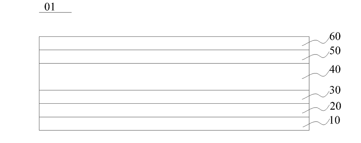
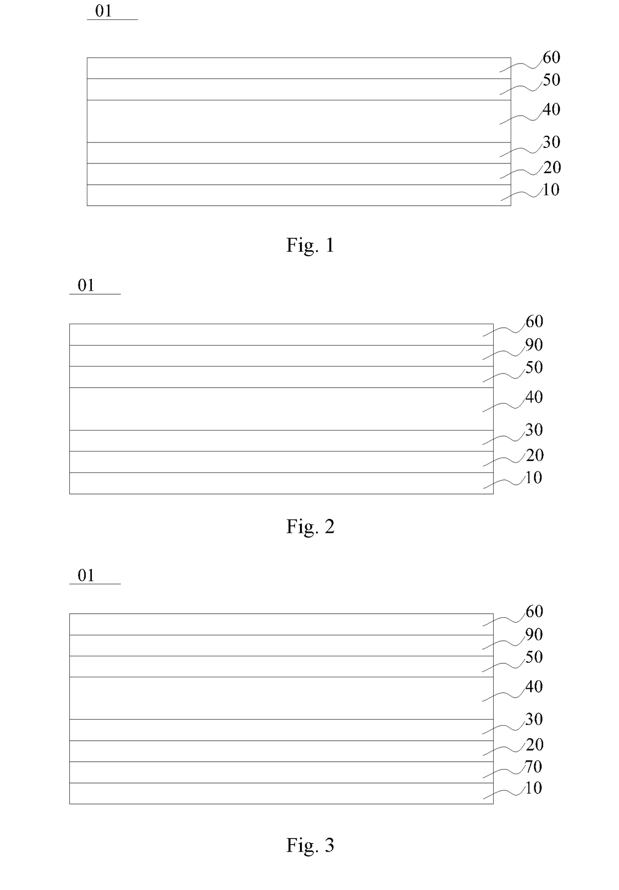
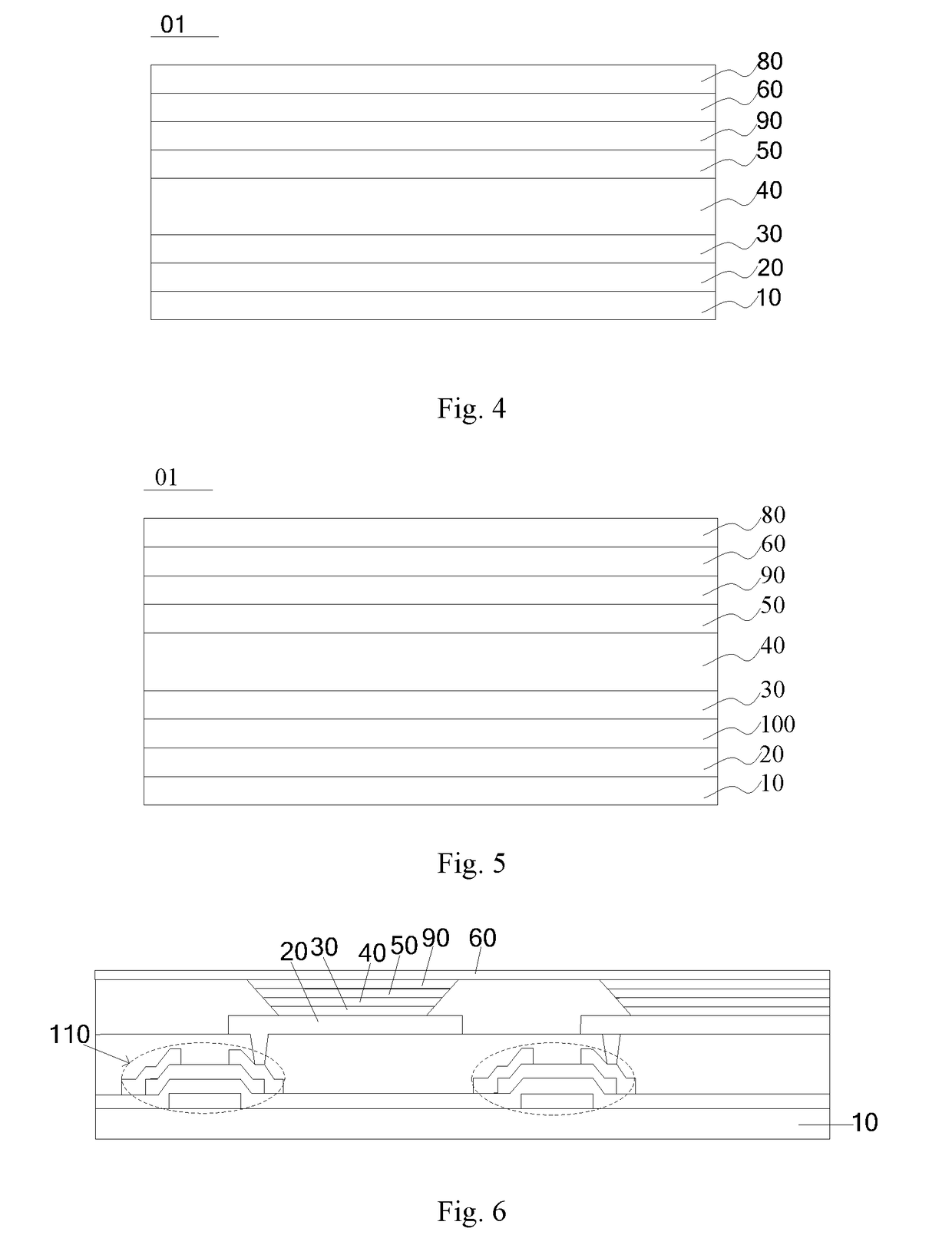
[0033]An embodiment of the disclosure provides an OLED light-emitting device 01. As shown in FIGS. 1-5, this OLED light-emitting device 01 comprises a substrate 10, and an anode 20, a hole transport layer 40, a blue light-emitting layer, and a cathode 60 provided on the substrate 10, and further comprises an Ag nanolayer 30 located between the anode 20 and the hole transport layer 40.

[0034]Here, the blue light-emitting layer is a blue phosphorescent light-emitting layer 50; and the abs...


PUM


Abstract

This disclosure provides an OLED light-emitting device, a production method thereof as well as a display apparatus, and relates to the technical field of OLED display, which can enhance the internal quantum efficiency of a blue OLED light-emitting device. This OLED light-emitting device comprises a substrate, and an anode, a hole transport layer, a blue light-emitting layer and a cathode provided on the substrate; the OLED light-emitting device further comprises an Ag nanolayer located between the anode and the hole transport layer; wherein the blue light-emitting layer is a blue phosphorescent light-emitting layer; the absorption spectrum of the Ag nanolayer overlaps the emission spectrum of the blue phosphorescent light-emitting layer, and the blue phosphorescent light-emitting layer is located within the penetration depth of surface plasma of Ag nanoparticles in the Ag nanolayer. It is used in the production of a blue OLED light-emitting device and a display apparatus comprising the same.

Description

FIELD OF THE INVENTION[0001]This disclosure relates to the technical field of OLED display, and particularly to an OLED light-emitting device and a production method thereof as well as a display apparatus.BACKGROUND OF THE INVENTION[0002]An organic light-emitting diode (simply referred to as OLED) has advantages of low energy consumption, high efficiency, spontaneous light emission, high response speed, or the like.[0003]A fluorescent or phosphorescent material is typically used as the luminescent material therein. Since the phosphorescent material still maintains a brightness for a considerable long period after excitation stops, the internal quantum efficiency thereof is higher than that of a known fluorescent material, OLEDs which mainly use the mechanism of phosphorescent light emission are highly anticipated recently.[0004]However, options of phosphorescent materials suitable for emitting blue light are relatively few at present, resulting in that the enhancement of the interna...

Claims


Application Information

Patent Timeline
Patent Type & Authority Applications(United States)
IPC IPC(8): H01L51/52H01L27/32H01L51/50H01L51/56
CPCH01L51/5293H01L27/3244H01L51/5206H01L51/5221H01L51/5016H01L51/5056H01L51/5265H01L51/5275H01L51/56H01L2251/301H01L2251/5369H01L2251/558H01L51/001H10K59/00H10K50/00H10K50/115H10K71/00H10K50/11H10K2101/10H10K50/852H10K50/856H10K2102/331H10K50/868H10K50/15H10K50/81H10K50/82H10K50/854H10K50/858H10K59/12H10K71/164H10K2102/00H10K2102/351
Inventor BAI, JUANJUANLAI, WEILINXUAN, MINGHUASUN, LIANG
Owner BOE TECH GRP CO LTD
Why Eureka
Try Eureka