

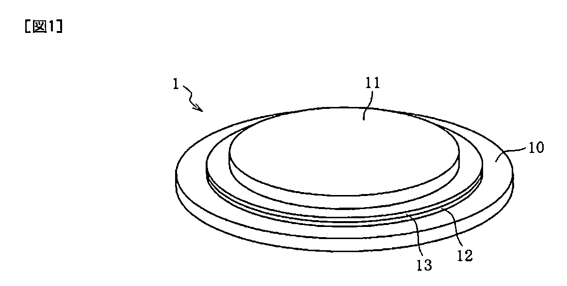
Supporting glass substrate, laminate, semiconductor package, electronic device, and method of manufacturing semiconductor package
a technology of supporting glass substrate and semiconductor package, which is applied in the direction of manufacturing tools, lapping machines, other domestic articles, etc., can solve the problems of difficult to increase the number of pins, high-density mounting of semiconductor chips, and strict mounting space for semiconductor chips to be used in those electronic devices, so as to reduce the variation of total thickness, the processing substrate is supported more accurately, and the effect of strong and accurate suppor
- Summary
- Abstract
- Description
- Claims
- Application Information
AI Technical Summary
Benefits of technology
Problems solved by technology
Method used
Image

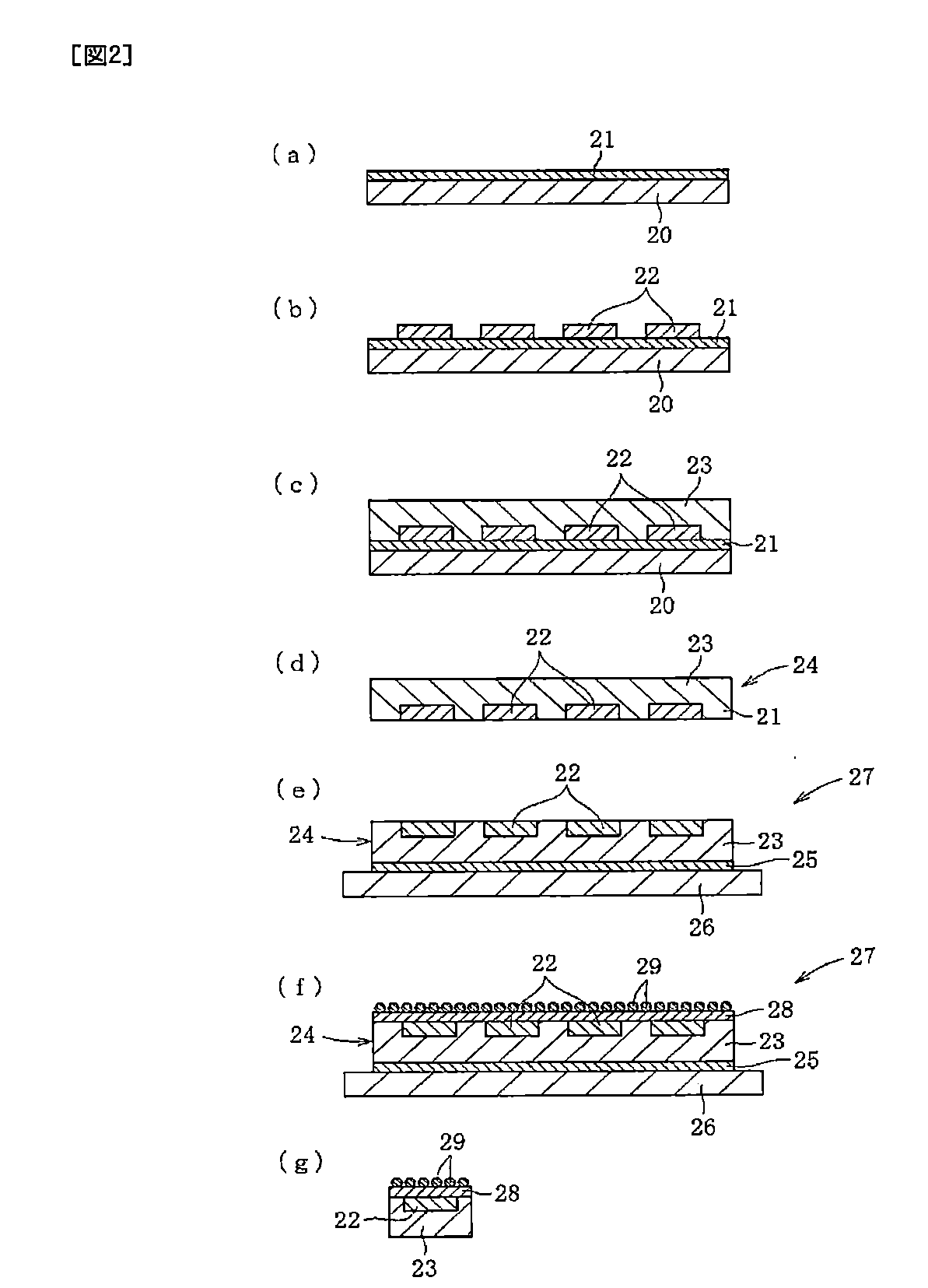
Examples
example 1
[0061]Now, the present invention is described with reference to Examples. However, Examples below are merely examples, and the present invention is by no means limited thereto.
[0062]Glass raw materials were blended so as to comprise as a glass composition, in terms of mass %, 65.7% of SiO2, 22% of Al2O3, 3.7% of Li2O, 0.3% of Na2O, 0.3% of K2O, 0.7% of MgO, 1% of BaO, 2% of TiO2, 2.7% of ZrO2, 1.4% of P2O5, and 0.2% of SnO2. After that, the resultant was loaded into a glass melting furnace to be melted at from 1,500° C. to 1,600° C. Then, the molten glass was supplied into a roll-out forming device so as to be formed to a thickness of 0.7 mm. Finally, the resultant was subjected to boring to be formed into a substantially disc shape. The obtained glass substrate was measured for an average thermal expansion coefficient within a temperature range of from 30° C. to 380° C. As a result, the average thermal expansion coefficient was 44×10−7 / ° C. Each of the obtained glass substrates (se...
example 2
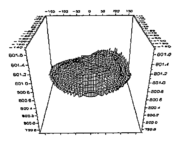
[0065]First, glass raw materials were blended so as to have a glass composition of each of Sample Nos. 1 to 7 shown in Table 3. After that, the resultant was loaded into a glass melting furnace to be melted at from 1,500° C. to 1,600° C. Then, the molten glass was supplied into an overflow down-draw forming device so as to be formed to a thickness of 0.8 mm. Each obtained glass substrate was evaluated for an average thermal expansion coefficient α30-380 within a temperature range of from 30° C. to 380° C., a density ρ, a strain point Ps, an annealing point Ta, a softening point Ts, a temperature at a viscosity at high temperature of 104.0 dPa·s, a temperature at a viscosity at high temperature of 103.0 dPa·s, a temperature at a viscosity at high temperature of 102.5 dPa·s, a temperature at a viscosity at high temperature of 102.0 dPa·s, a liquidus temperature TL, and a Young's modulus E. Each glass substrate after forming was measured for a total thickness variation and a warpage le...
PUM
| Property | Measurement | Unit |
|---|---|---|
| Length | aaaaa | aaaaa |
| Thickness | aaaaa | aaaaa |
| Thickness | aaaaa | aaaaa |
Abstract
Description
Claims
Application Information