Spiral and concentric movement designed for cmp location specific polish (LSP)

Inactive Publication Date: 2018-09-06
APPLIED MATERIALS INC
View PDF31 Cites 4 Cited by
  • Summary
  • Abstract
  • Description
  • Claims
  • Application Information

AI Technical Summary

Benefits of technology

The patent describes methods for polishing semiconductor wafers using a polishing pad with a small contact surface area. The methods involve polishing the substrate with a first polishing recipe, then moving the polishing pad to a second radius on the substrate and polishing it with a second polishing recipe. This results in a planarized surface without dishing of the material filling holes or trenches. In addition, the patent describes a method for determining the residual film thickness profile of the substrate and generating polishing recipes based on it. The technical effects of the patent include improved planarization of substrate surfaces and more efficient polishing of semiconductor wafers.

Problems solved by technology

The smoothing effect makes local pressure application, for local material removal, difficult if not impossible.
However, post-CMP, the film thickness, and film removal rate, of a substrate may be non-uniform thereacross as a degree of non-uniform material removal across the substrate is inherent in most conventional CMP processes.
Thus, reworking of a substrate where the polished layer is too thick or has an undesired residual film thereon may result in film that is too thin at some locations or locations that are over-polished during the rework operation.
In addition to over-polish resulting in a film thickness that is too thin, over-polishing may result in undesirable dishing of the upper surface of a film material in recessed features such as vias, contacts and lines, and / or erosion of the planer surface in areas with high feature density.
In addition, over-exposure of a metal such as tungsten (W) to the a metal CMP slurry can result in chemical conversion of the metal by the slurry and thus coring, where the metal fill material no longer adheres to the side wall and base of the opening which it fills, and it pulls away during polishing.

Method used


Image

  • Spiral and concentric movement designed for cmp location specific polish (LSP)
  • Spiral and concentric movement designed for cmp location specific polish (LSP)
  • Spiral and concentric movement designed for cmp location specific polish (LSP)

Examples


Embodiment Construction

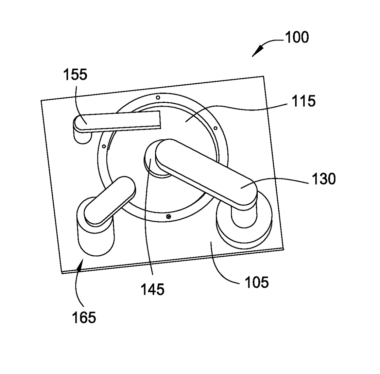
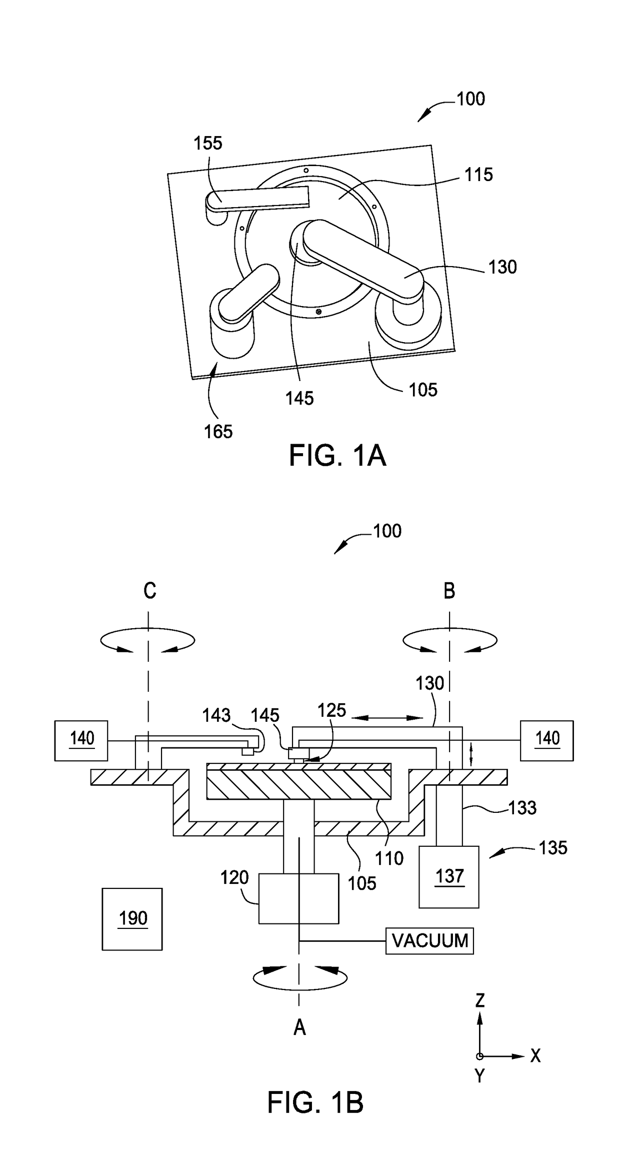
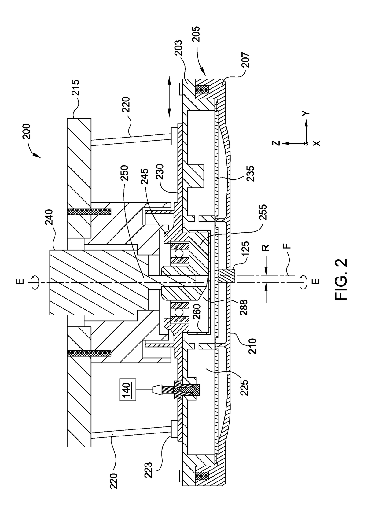
[0028]The present disclosure provides a method of polishing a film layer on a substrate using a module particularly suited for location specific polishing (LSP) on the substrate during a fabrication process. The method includes the generation of a thickness correction profile for a film layer on the substrate and the generation of a polishing recipe, or series of polishing recipes, based on the thickness correction profile. In some embodiments, the method may be employed before or after a conventional CMP operation. When the method is used before a conventional CMP operation, in one aspect it is used to selectively remove film layer material, by polishing portions of the exposed film layer, to correct for the existing non-uniform film thickness thereof, and / or to selectively remove film layer material, by polishing portions of the exposed film layer, in anticipation of non-uniform removal of portions of the film layer material during conventional CMP. When the method is used after a...


PUM


Abstract

A method is provided to minimize travel distance and time between correction locations on a substrate when polishing a local area of a substrate, such as a semiconductor wafer, using a location specific polishing module. A correction profile is determined and a recipe based on the correction profile is used to polish a substrate. A polishing pad assembly traverses between a first correction location and a second correction location using the combined motion of a substrate support chuck and a support arm coupled at a first end thereof to the polishing pad assembly. The chuck rotates about a center axis thereof. The positioning arm may sweep about a vertical axis disposed through a second end of the support arm. The combined motion of the chuck and the positioning arm causes the polishing pad assembly to form a spiral shaped polishing path on the substrate.

Description

CROSS REFERENCE TO RELATED APPLICATIONS[0001]This application claims priority to U.S. Provisional Patent Application Ser. No. 62 / 467,672 filed Mar. 6, 2017 which is herein incorporated by reference in its entirety.BACKGROUNDField[0002]Embodiments of the present disclosure generally relate to methods for polishing a substrate, such as a semiconductor wafer, and more particularly, to methods for polishing specific locations or regions of a substrate in an electronic device fabrication process.Description of the Related Art[0003]Chemical mechanical polishing (CMP) is a process which is commonly used in the manufacture of high-density integrated circuits to planarize or polish a layer of material deposited on a substrate, by contacting the material layer to be planarized with a polishing pad and moving the substrate, and hence the material layer surface, with respect to the polishing pad in the presence of a polishing fluid such as a slurry. In a typical polishing process, the substrate...

Claims


Application Information

Patent Timeline
IPC IPC(8): B24B7/22B24B13/005B24B49/10B24B37/07
CPCB24B7/228B24B13/005B24B49/10B24B37/07H01L21/304H01L21/30625H01L21/31053H01L21/3212H01L22/20B24B37/005B24B37/042
Inventor LAU, ERICCHOU, CHIH CHUNGGARRETSON, CHARLES C.OH, JEONGHOONHEUNG, KING YI
Owner APPLIED MATERIALS INC
Why Eureka
Try Eureka