Silicon carbide semiconductor device and method of manufacturing silicon carbide semiconductor device
- Summary
- Abstract
- Description
- Claims
- Application Information
AI Technical Summary
Benefits of technology
Problems solved by technology
Method used
Image

Examples
embodiments
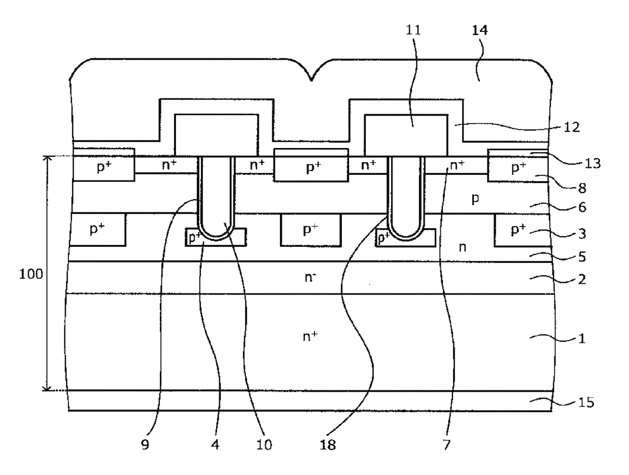
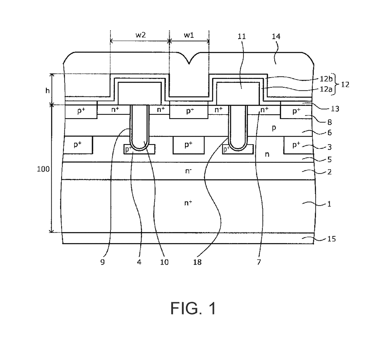
[0048]A semiconductor device of the present embodiment is formed using a semiconductor with a wider bandgap than silicon (hereinafter, wide bandgap semiconductor). The structure of a semiconductor device (silicon carbide semiconductor device) that uses silicon carbide (SiC), for example, as the wide bandgap semiconductor will be described as an example. FIG. 1 is a cross-sectional view of a structure of a silicon carbide semiconductor device according to the embodiment. FIG. 1 shows only two unit cells (functional units of the device), and the other unit cells adjacent to these unit cells are not shown in the drawings. The silicon carbide semiconductor device according to the embodiment shown in FIG. 1 is a MOSFET including a MOS gate on the front surface (p-type base layer 6 side surface) side of a semiconductor substrate made of silicon carbide (silicon carbide substrate: semiconductor chip).
[0049]The silicon carbide substrate 100 is formed by epitaxially growing an n− drift regio...
PUM
 Abstract
Description
Claims
Application Information
 - R&D Engineer
- R&D Manager
- IP Professional
- Industry Leading Data Capabilities
- Powerful AI technology
- Patent DNA Extraction
Browse by: Latest US Patents, China's latest patents, Technical Efficacy Thesaurus, Application Domain, Technology Topic.
© 2024 PatSnap. All rights reserved.Legal|Privacy policy|Modern Slavery Act Transparency Statement|Sitemap