

Method of forming semiconductor device
a semiconductor and device technology, applied in semiconductor/solid-state device manufacturing, basic electric elements, electric devices, etc., can solve the problems of affecting the quality of the product in the subsequent metallization process, and improving the possibility of defects generated during the damascene process, so as to achieve better yield and quality, yield and quality. good
- Summary
- Abstract
- Description
- Claims
- Application Information
AI Technical Summary
Benefits of technology
Problems solved by technology
Method used
Image

Examples
Embodiment Construction
[0020]To provide a better understanding of the presented invention, preferred embodiments will be described in detail. The preferred embodiments of the present invention are illustrated in the accompanying drawings with numbered elements.
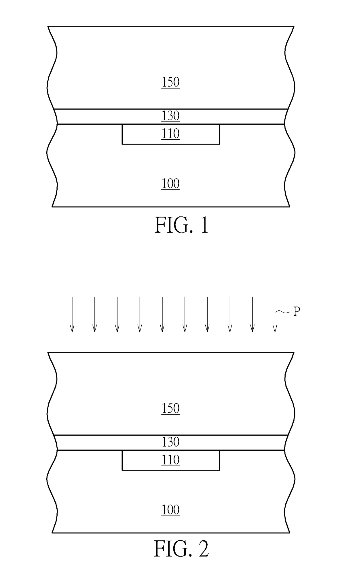
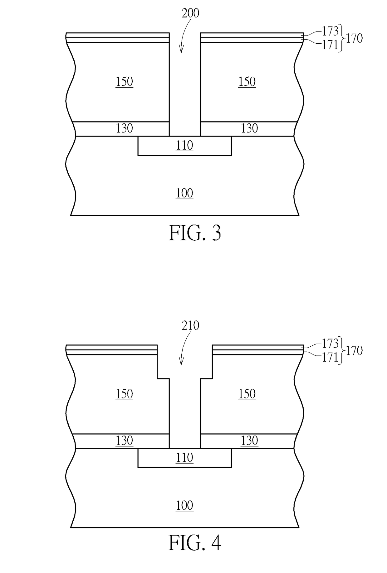
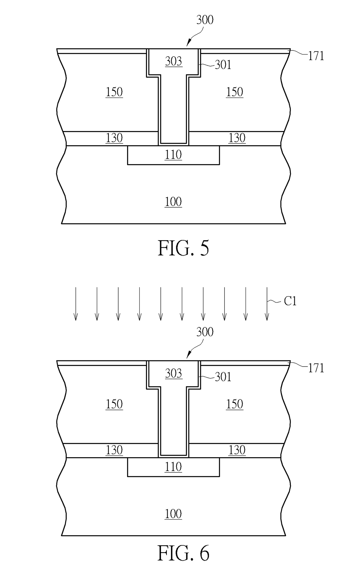
[0021]Please refer to FIG. 1 to FIG. 7, which are schematic diagrams illustrating a forming process of a semiconductor device according to the first embodiment of the present invention. First of all, a substrate layer 100 is provided and a conductive layer 110 is formed either in the substrate layer 100 as shown in FIG. 1 or on the substrate layer 100 (not shown in the drawings). In the present embodiment, the substrate layer 100 is a dielectric layer for example including silicon oxide (SiO2) disposed on a semiconductor substrate (not shown in the drawings) such as a silicon substrate, a silicon germanium substrate or a silicon-on-insulator (SOI) substrate, and the conductive layer 110 is a via plug or a metal line formed in the substrate layer 100...
PUM
 Abstract
Description
Claims
Application Information