Epitaxial structure of n-face group iii nitride, active device, and method for fabricating the same with integration and polarity inversion

Active Publication Date: 2018-12-06
HUANG CHIH SHU
View PDF10 Cites 16 Cited by
  • Summary
  • Abstract
  • Description
  • Claims
  • Application Information

AI Technical Summary

Benefits of technology

[0002]According to the prior art, the most common structures to achieve an enhancement-mode AlGaN/GaN high electron mobility transistor (E-mode AlGaN/GaN HEMT) include: 1. Ga-face p-GaN gate E-mode HEMT structure, and 2. N-face AlxGaN gate E-mode HEMT structure. Nonetheless, as implied by their names, only the gate region will be p-GaN or AlxGaN.
[0003]The most common fabrication method is to grow an additional P-GaN layer on the tradition epitaxial structure of depletion-mode (D-mode) AlGaN/GaN HEMT. Afterwards, etch p-GaN outside the gate region using dry etching while maintaining the completeness of the thickness of the underlying epitaxial layer. Because if the underlying epitaxial layer is etched too much, the two-dimensional electron gas (2DEG) will not be formed at the interface AlGaN/GaN of a Ga-face p-GaN gate E-mode HEMT structure. Thereby, using dry etching is challenging because the etching depth is hard to control and nonuniformity in thickness still occurs in every epitaxial layer of an epitaxial wafer. Besides, both this epitaxial structure and the normal D-Mode AlGaN/GaN HEMT epitaxial structure face the problems related to current collapse, such as buffer traps and surface traps, requiring further resolution.
[0004]Accordingly, to improve the above drawbacks, the present invention provides a novel epitaxial structure of N-face group III nitride, an active device formed by using the epitaxial structure after polarity inversion, and the fabrication method for integration.
[0005]An objective of

Problems solved by technology

Thereby, using dry etching is challenging because the etching depth is hard to control and nonuniformity in thickness still occurs in every epitaxial layer of an epitaxial wafer.
Besides, both thi

Method used


Image

  • Epitaxial structure of n-face group iii nitride, active device, and method for fabricating the same with integration and polarity inversion
  • Epitaxial structure of n-face group iii nitride, active device, and method for fabricating the same with integration and polarity inversion
  • Epitaxial structure of n-face group iii nitride, active device, and method for fabricating the same with integration and polarity inversion

Examples


first embodiment

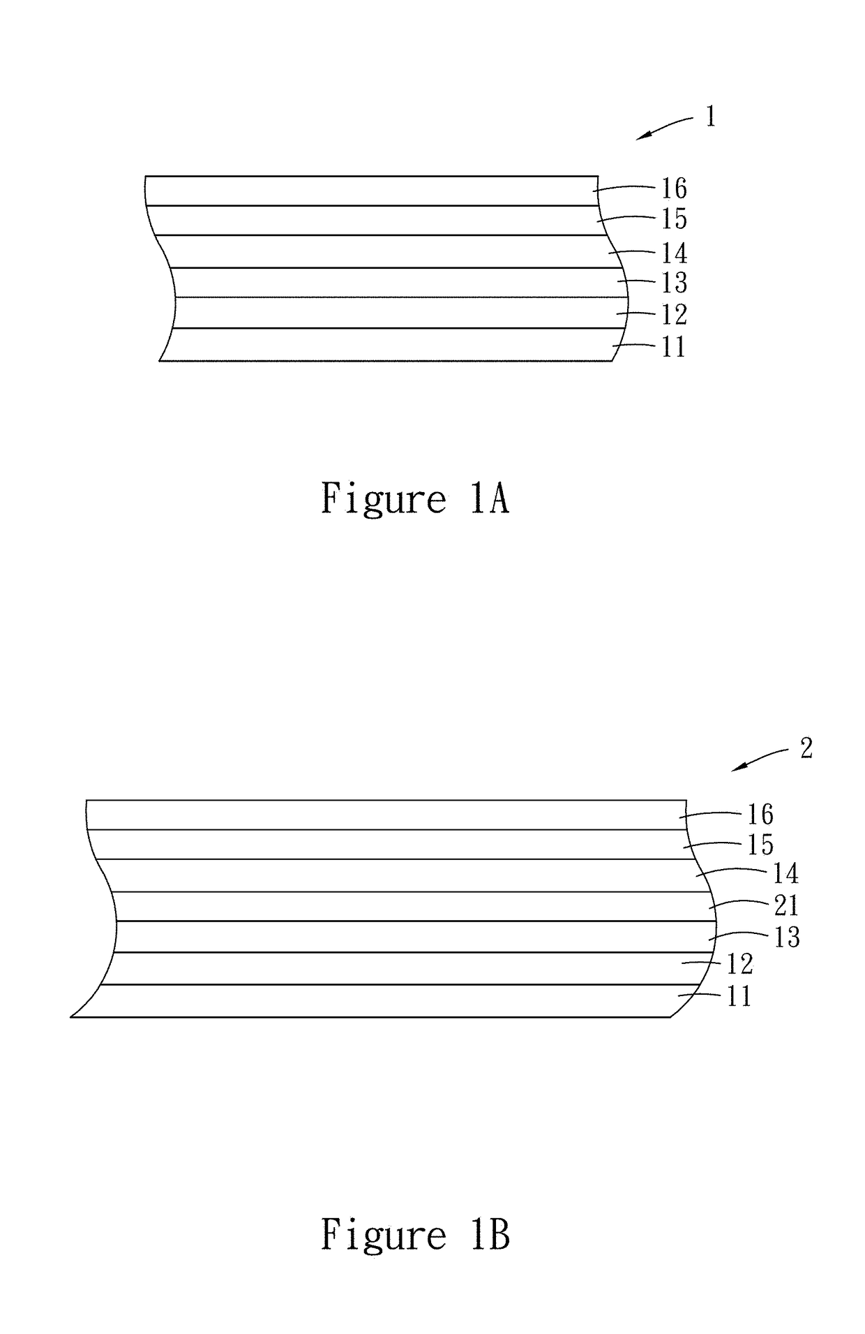
[0054]According to the present invention, the structures of FIGS. 1A and 1B can be further applied in fabricating a fluorine-ion-implanted E-mode N-face AlGaN / GaN HEMT with polarity inversion and gate moat structure.

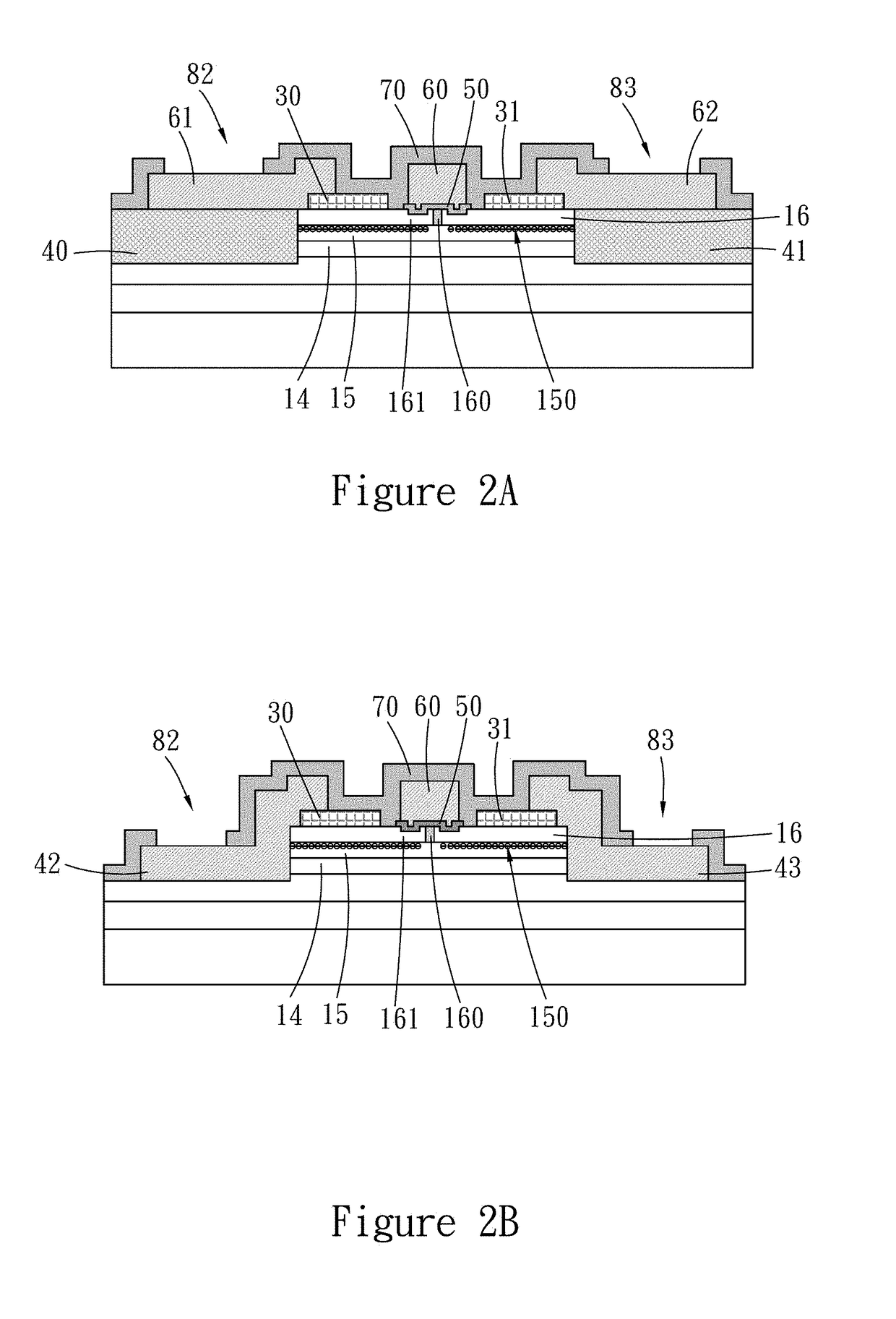
[0055]FIG. 2A shows a first structural schematic diagram of E-mode N-face AlGaN / GaN HEMT with polarity inversion (namely, generating stress by the passivation dielectric layer) by implanting fluorine ions into the i-AlxGaN layer 16 according to the present invention. As shown in the figure, the E-mode N-face AlGaN / GaN HEMT with polarity inversion according to the present invention is characterized in including the epitaxial structures 1 (as shown in FIG. 1A), 2 (as shown in FIG. 1B) of N-face AlGaN / GaN and the fluorine-on structure 160 located in the i-AlxGaN layer 16. Although the 2DEG 150 is formed in the i-GaN channel layer 15 at the junction between the i-AlxGaN layer 16 and the i-GaN channel layer 15, due to the existence of the fluorine-ion structure 160, the 2DEG ...

second embodiment

[0068]The FIG. 5A and FIG. 5B show a first and a second structure diagram of a hybrid E-mode N-face AlGaN / GaN HEMT with polarity inversion formed by cascoding an E-mode N-face AlGaN / GaN HEMT with polarity inversion and gate moat structure and a D-mode N-face AlGaN / GaN HEMT with polarity inversion and without gate dielectric layer according to the present invention. As shown in the figures, the dry etching method is adopted for etching the two gate moat structures 161 on the i-AlxGaN layer 16 on both sides of the predetermined location for the fluorine-ion structure 160. Next, fluorine ions are implanted into the i-AlxGaN layer 16 below the first gate electrode 60 to form a hybrid E-mode N-face AlGaN / GaN HEMT with polarity inversion formed by cascoding an E-mode N-face AlGaN / GaN HEMT with polarity inversion and gate moat structure and a D-mode N-face AlGaN / GaN HEMT with polarity inversion and without gate dielectric layer.

[0069]The hybrid E-mode AlGaN / GaN HEMT according to the prese...

third embodiment

[0083]Please refer to FIG. 6A and FIG. 6B, which show a first and a second structure diagram of a hybrid E-mode N-face AlGaN / GaN HEMT with polarity inversion formed by cascoding an E-mode N-face AlGaN / GaN HEMT with polarity inversion and gate moat structure and a D-mode N-face AlGaN / GaN HEMT with polarity inversion and gate dielectric layer according to the present invention. As shown in the figures, according to the present invention, fluorine ions are implanted into the i-AlxGaN layer 16 (x=0.1˜0.3) below the first gate electrode 60 to form a hybrid E-mode N-face AlGaN / GaN HEMT with polarity inversion formed by cascoding an E-mode N-face AlGaN / GaN HEMT with polarity inversion and gate moat structure and a D-mode N-face AlGaN / GaN HEMT with polarity inversion and gate dielectric layer 50.

[0084]As shown in FIGS. 6A and 6B, the hybrid E-mode AlGaN / GaN HEMT with polarity inversion according to the third embodiment includes the device structure of the epitaxial structure of N-face AlGaN...


PUM


Abstract

The present invention provides an epitaxial structure of N-face group III nitride, its active device, and the method for fabricating the same. By using a fluorine-ion structure in device design, a 2DEG in the epitaxial structure of N-face group III nitride below the fluorine-ion structure will be depleted. Then the 2DEG is located at a junction between a i-GaN channel layer and a i-AlyGaN layer, and thus fabricating GaN enhancement-mode AlGaN/GaN high electron mobility transistors (HEMTs), hybrid Schottky barrier diodes (SBDs), or hybrid devices. After the fabrication step for polarity inversion, namely, generating stress in a passivation dielectric layer, the 2DEG will be raised from the junction between the i-GaN channel layer and the i-AlyGaN layer to the junction between the i-GaN channel layer and the i-AlxGaN layer.

Description

FIELD OF THE INVENTION[0001]The present invention relates generally to an epitaxial structure, and particularly to an epitaxial structure of N-face (Nitride-Face) group III nitride grown in series on semiconductors. The advantage of the present invention is that i-AlxGaN grown on the N-face polarity will have less defects. By using the fabrication method according to the present invention, namely, by taking advantages of the stress generated by the passivation dielectric layer, the N-face polarity can be inverted to the Ga-face polarity. Thereby, the 2DEG can be transferred from the interface of i-GaN / i-AlyGaN in the i-GaN channel layer to the interface of i-AlxGaN / i-GaN in the i-GaN channel layer. In addition to giving lower i-AlxGaN surface traps, while the i-AlyGaN became the role of blocking buffer trap electrons from entering the channel layer, and hence easing the problem of current collapse. Furthermore, the present invention also provides a gate moatmoat structure located in...

Claims


Application Information

Patent Timeline
IPC IPC(8): H01L29/66C30B25/04C30B29/40H01L21/02H01L29/10H01L29/778
CPCH01L29/66462C30B25/04C30B29/406H01L21/02381H01L21/02458H01L29/1066H01L29/1075H01L29/7781H01L29/7783H01L21/8252H01L27/0629C30B25/183H01L29/402H01L29/4236H01L29/42376H01L29/66212H01L29/7786H01L27/0605H01L29/872H01L29/205H01L29/207H01L21/823412H01L21/823462H01L27/085
Inventor HUANG, CHIH-SHU
Owner HUANG CHIH SHU
Why Eureka
Try Eureka