Inductor and method for manufacturing the same

a technology of inductor electrodes and manufacturing methods, which is applied in the direction of transformers/inductances, inductances, magnetic cores of transformers/inductances, etc., can solve the problems of reducing the resistance of the entire inductor electrode, unable to meet the enhancement of multifunctionality, and the structure may fail to meet the requirements of size reduction and enhancement of multifunctionality, etc., to achieve low specific resistance, low cost, and easy manufacturing

Active Publication Date: 2018-12-20
MURATA MFG CO LTD
View PDF2 Cites 7 Cited by
  • Summary
  • Abstract
  • Description
  • Claims
  • Application Information

AI Technical Summary

Benefits of technology

[0018]With this method, an inductor that includes an inductor electrode including metal pins and metal boards having lower specific resistance than conductive paste or plating can be easily manufactured. This structure does not include a filled via as a portion of the inductor electrode, so that an inductor having desired characteristics such as inductance can be manufactured at low costs. To form, in a resin layer, an inductor electrode of a multiplex winding structure including an inner winding portion and an outer winding portion, an existing method involves, for example, forming portions corresponding to first and second metal boards of the inner winding portion on both main surfaces of a first resin layer, and then forming other resin layers between these metal boards and third and fourth metal boards of the outer winding portion. However, a method for manufacturing an inductor according to the present disclosure only requires forming a single resin layer. Forming insertion holes with a large diameter in the third and fourth metal boards constituting a part of the outer winding portion enable

Problems solved by technology

Reducing the resistance of the entire inductor electrode is thus difficult.
This structure thus m

Method used


Image

  • Inductor and method for manufacturing the same
  • Inductor and method for manufacturing the same
  • Inductor and method for manufacturing the same

Examples


first embodiment

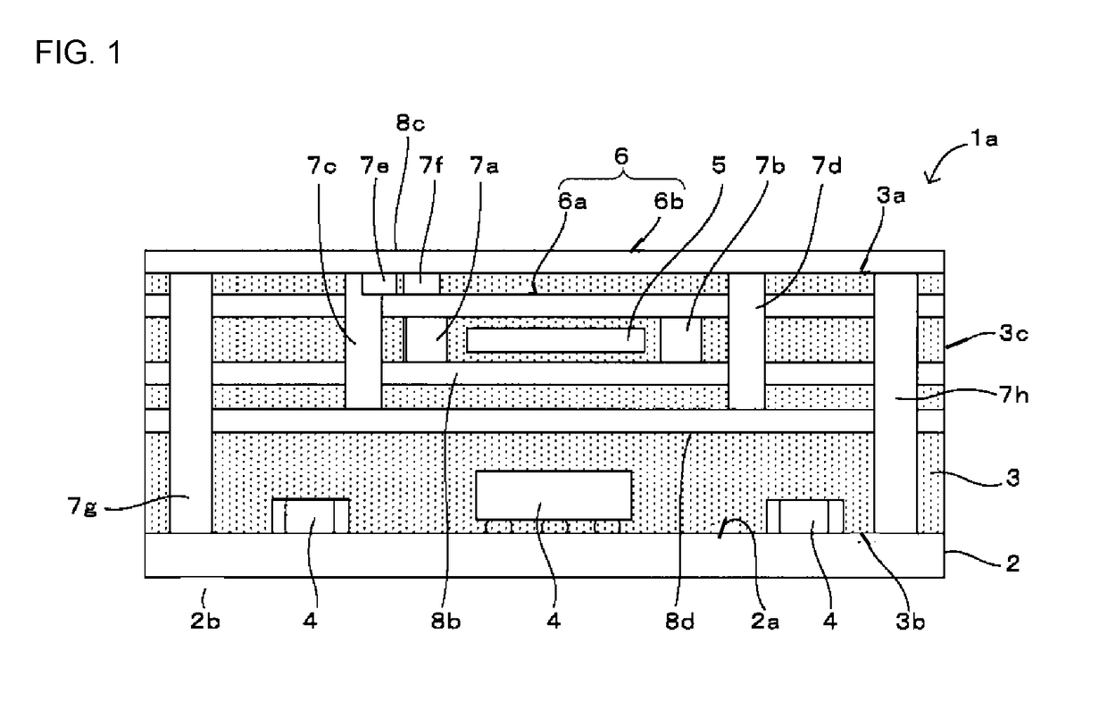
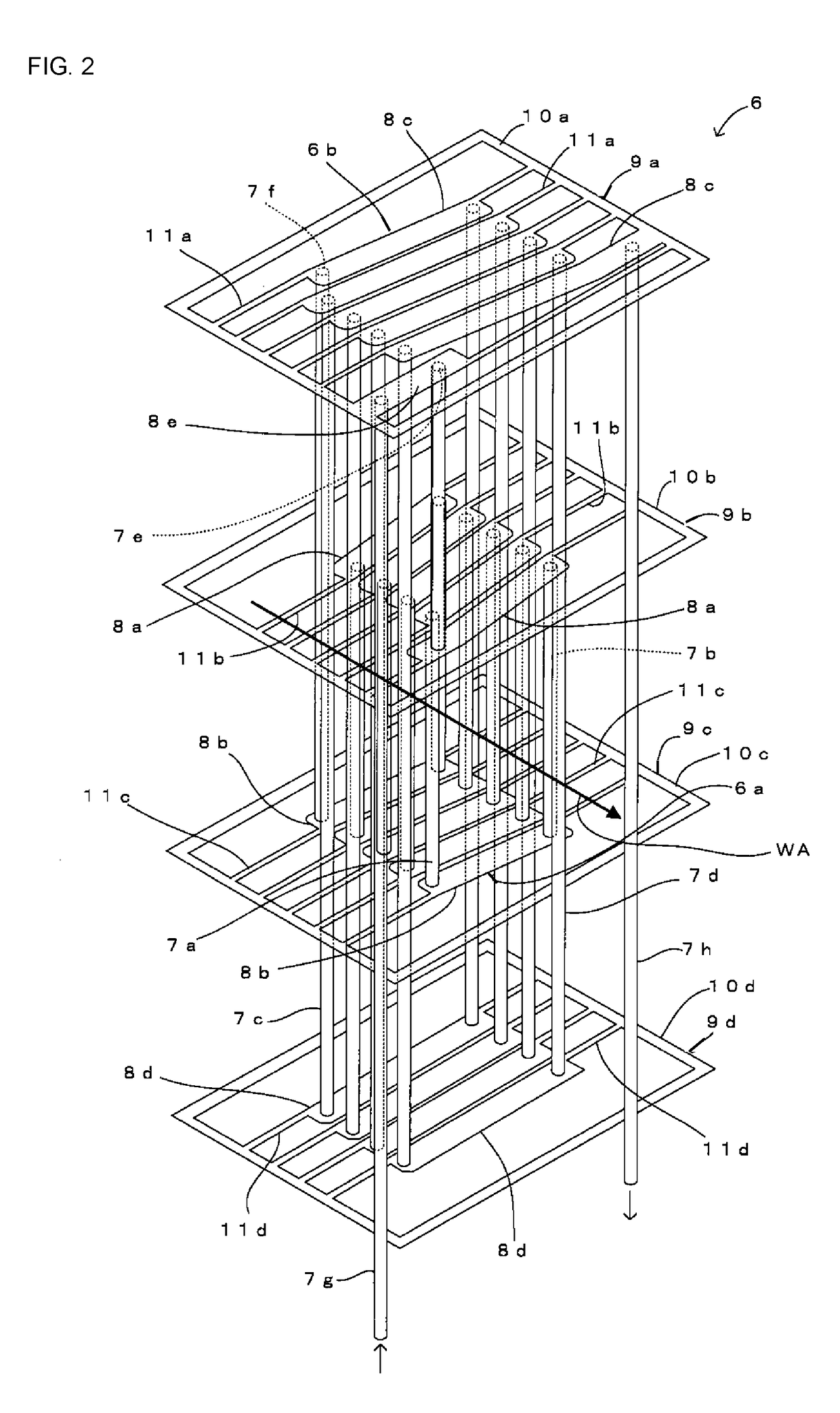
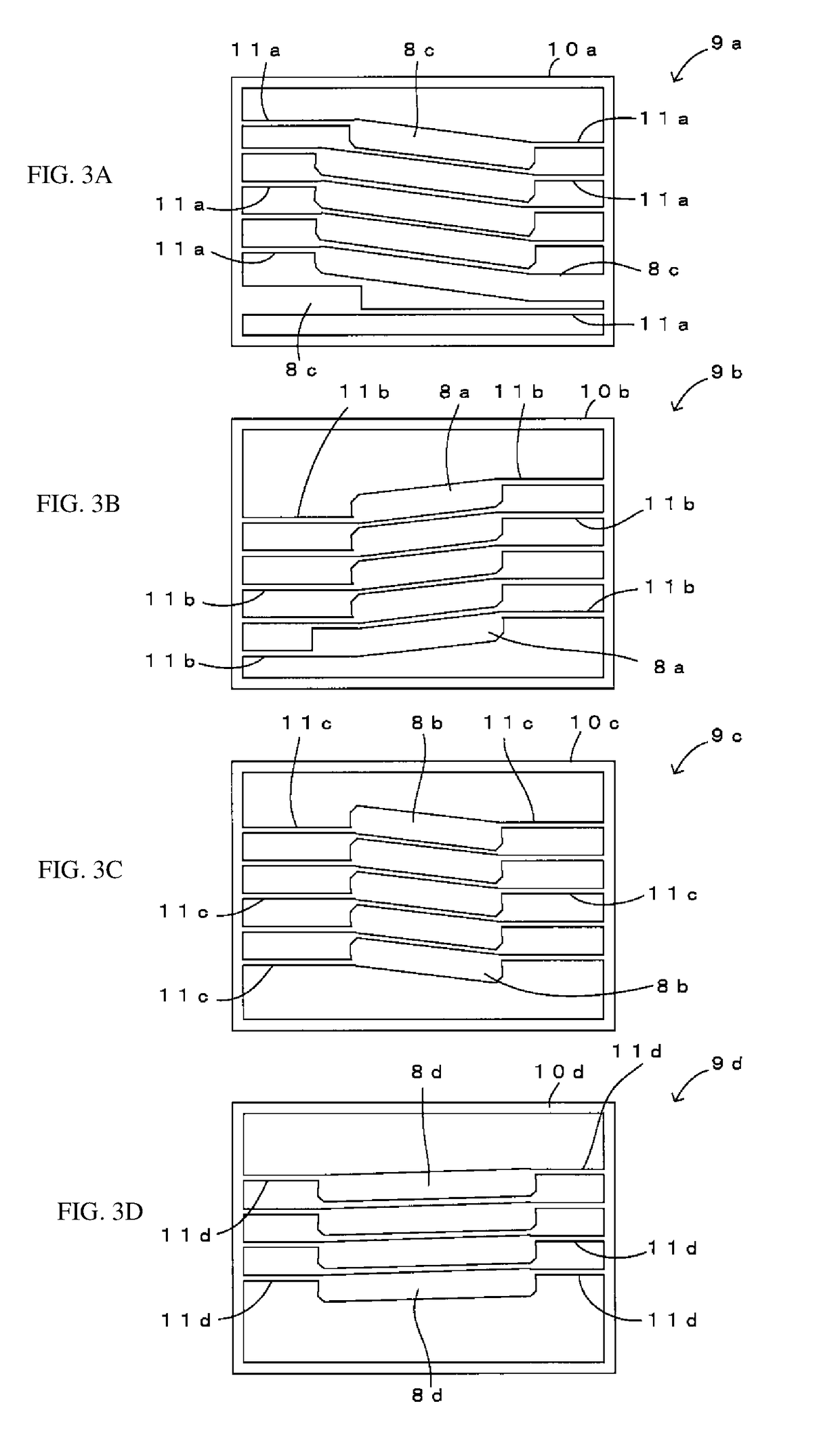
[0034]An inductor according to a first embodiment of the present disclosure is described with reference to FIG. 1 to FIG. 3D. FIG. 1 illustrates the inductor viewed in a direction parallel to the main surface of the circuit board and omits illustration of a part of a resin layer to show the internal structure. FIG. 2 is a perspective view of an inductor electrode and illustrates a wiring structure. FIG. 3A is a plan view of an outer-winding upper wiring board, FIG. 3B is a plan view of an inner-winding upper wiring board, FIG. 3C is a plan view of an inner-winding lower wiring board, and FIG. 3D is a plan view of an outer-winding lower wiring board.

[0035]An inductor 1a according to the present embodiment includes a circuit board 2, a resin layer 3, laminated on an upper surface 2a or a first main surface of the circuit board 2, multiple components 4, mounted on the upper surface 2a of the circuit board 2, a coil core 5, disposed inside the resin layer 3, and an inductor electrode 6....

second embodiment

[0070]An inductor according to a second embodiment of the present disclosure is described with reference to FIG. 7. FIG. 7 illustrates an inductor of the second embodiment and corresponds to FIG. 1.

[0071]An inductor 1b according to the present embodiment differs from the inductor 1a according to the first embodiment described with reference to FIG. 1 in that, as illustrated in FIG. 7, main surfaces 2a and 2b of the circuit board 2 have smaller areas, the side surfaces of the circuit board 2 are covered with the resin layer 3, and the lower end surfaces of the input metal pin 7g and the output metal pin 7h are exposed from the lower surface 3b of the resin layer 3. Other components are the same as those of the inductor 1a according to the first embodiment, and thus are denoted with the same reference signs and not described.

[0072]Besides the effects of the first embodiment, this structure allows the inductor electrode 6 to be directly connected to the mother board.

third embodiment

[0073]An inductor according to a third embodiment of the present disclosure is described with reference to FIG. 8 and FIGS. 9A to 9D. FIG. 8 illustrates an inductor according to this embodiment, and corresponds to FIG. 1. FIGS. 9A to 9D include plan views of wiring boards supported by frames, and correspond to FIGS. 3A to 3D.

[0074]An inductor 1c according to the present embodiment differs from the inductor 1a according to the first embodiment described with reference to FIG. 1 in that, as illustrated in FIG. 8, an inductor electrode 60 has a different structure, the components 4 are disposed at different positions, and a support plate 13 is additionally included. Other components are the same as those of the inductor 1a according to the first embodiment, and thus are denoted with the same reference signs and not described.

[0075]Here, the metal pins 7a to 7h constituting a part of the inductor electrode 60 have the same length and the same thickness, and have their upper end surfaces...


PUM


Abstract

A small-sized inductor with desired characteristics is provided. An inductor 1a includes a resin layer 3 and an inductor electrode 6, which includes an inner winding portion 6a and an outer winding portion 6b. The inner winding portion 6a and the outer winding portion 6b forming the inductor electrode 6 include the metal pins 7a to 7d and the wiring boards 8a to 8d. Here, the inner winding portion 6a and the outer winding portion 6b include the metal pins 7a to 7d and the wiring boards 8a to 8d, which have lower specific resistance than conductive paste or plating. This structure thus can reduce the resistance of the entirety of the inductor electrode 6, and improve the characteristics of the inductor 1a. The inductor 1a can reduce its size by including the inductor electrode 6 wound to have a multiplex winding structure.

Description

[0001]This is a continuation of International Application No. PCT / JP2016 / 078772 filed on Sep. 29, 2016 which claims priority from Japanese Patent Application No. 2016-026777 filed on Feb. 16, 2016. The contents of these applications are incorporated herein by reference in their entireties.BACKGROUND OF THE DISCLOSUREField of the Disclosure[0002]The present disclosure relates to an inductor including a resin layer and an inductor electrode, and a method for manufacturing the same.Description of the Related Art[0003]An inductor 100, illustrated in FIG. 14, including a coil 102 in a core substrate 101 formed from a printed circuit board or a prepreg is known (see, for example, Patent Document 1). In this case, an annular magnetic layer 103 is disposed in the core substrate 101, and the coil 102 is helically wound around the magnetic layer 103. The coil 102 includes multiple internal interlayer connection conductors 102a, arranged along the inner periphery of the magnetic layer 103, mul...

Claims


Application Information

Patent Timeline
IPC IPC(8): H01F27/29H05K1/18H01F27/24H01F27/28H01F41/04H05K3/30
CPCH01F27/29H05K1/185H01F27/24H01F27/28H01F41/04H05K3/30H05K2201/1003H05K2203/1305H01F17/0033H05K1/165
Inventor OTSUBO, YOSHIHITONISHIDE, MITSUYOSHISAKAI, NORIO
Owner MURATA MFG CO LTD
Why Eureka
Try Eureka