

Printing plate, method for manufacturing printing plate, and printing method
- Summary
- Abstract
- Description
- Claims
- Application Information
AI Technical Summary
Benefits of technology
Problems solved by technology
Method used
Image

Examples
example 1
Evaluation of Example 1
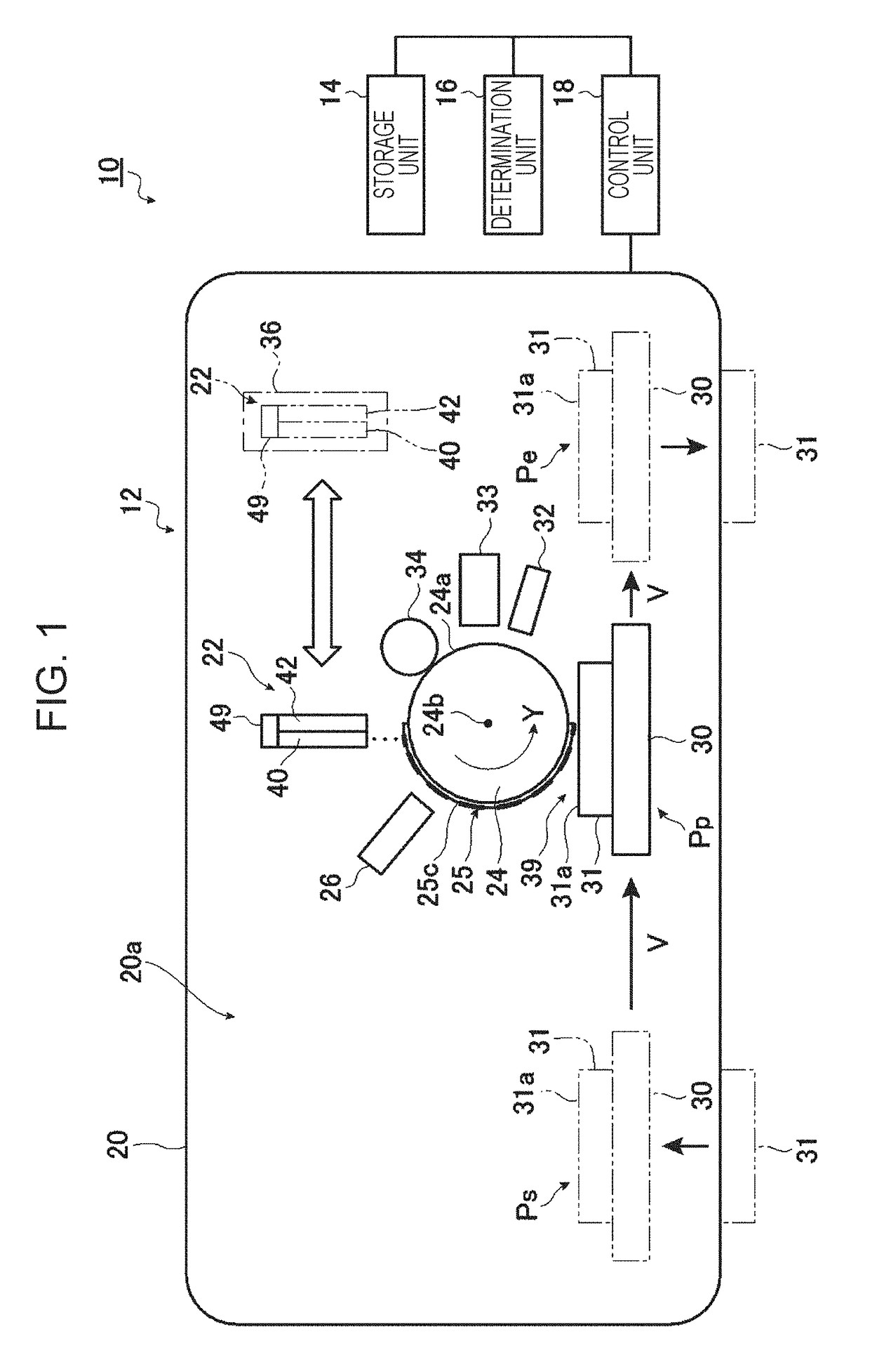
[0316]The surface structure of the printing plate was evaluated under a scanning probe microscope. The results are shown in FIGS. 19 and 20.
[0317]As shown in FIG. 19, the printing plate 25 had the image area 25a and the non-image area 25b formed thereon. As shown in FIG. 20, the height difference between the image area 25a and the non-image area 25b was about 10 nm. In addition, there were projections 25d on the boundaries between the image area 25a and the non-image area 25b.
[0318]The advancing contact angles θA,s and the receding contact angles θR,f of the image area 25a, that is, the ink-receptive area, and the non-image area 25b, that is, the ink-repellent area, of the printing plate 25 were measured by the tilting-plate method. In addition, a printing test was performed on a polycarbonate film by inking with the pigment ink having silver nanoparticles dispersed therein using an inkjet apparatus (available from Dimatix, Inc., 10 pL (picoliter) head).
[0319...
example 2
[0323]In this example, five samples, namely, Samples 1 to 5, were fabricated in the same manner as the printing plate of Example 1 above as follows.
[0324]Specifically, a silicone rubber layer cured by heating was subjected to activation treatment by irradiation with ultraviolet light using as a light source a VUS-3150 available from Orc Manufacturing Co., Ltd., which was equipped with an excimer lamp, in a nitrogen atmosphere with an oxygen concentration of less than 1% for 10 seconds.
[0325]Thereafter, a primer intended for Durasurf (DS-PC-3B (model No.)), serving as a silane coupling agent, was used to complete silane coupling treatment. Thereafter, any unreacted silane coupling agent was removed by spinning on a spin coater. Thereafter, five different levels of the fixing condition of the silane coupling agent were tested by changing the heating temperature and other heating conditions. Durasurf (DS-5210TH (product name)) available from Harves Co., Ltd., serving as a fluorine comp...
PUM
| Property | Measurement | Unit |
|---|---|---|
| Viscosity | aaaaa | aaaaa |
| Viscosity | aaaaa | aaaaa |
| Height | aaaaa | aaaaa |
Abstract
Description
Claims
Application Information